FinFET formation with a thermal oxide spacer hard mask formed from crystalline silicon layer
a technology of thermal oxide spacer and hard mask, which is applied in the direction of semiconductor devices, electrical equipment, decorative arts, etc., can solve the problems of non-uniform spacer width, inability to fabricate fin structures with tight or narrow pitches, and inability to control leakage currents
- Summary
- Abstract
- Description
- Claims
- Application Information
AI Technical Summary
Benefits of technology
Problems solved by technology
Method used
Image

Examples
Embodiment Construction
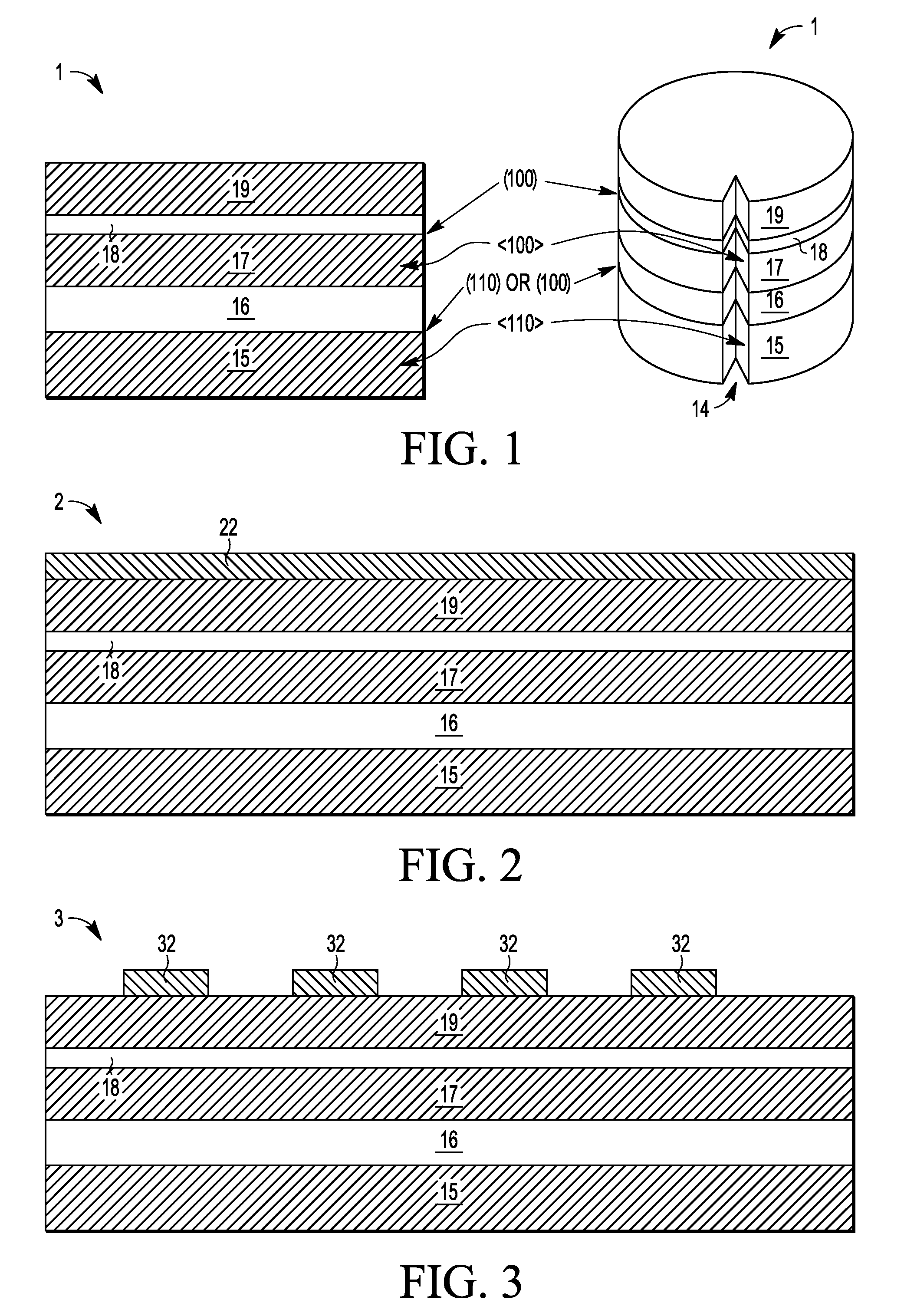
ill be appreciated that for simplicity and clarity of illustration, elements illustrated in the drawings have not necessarily been drawn to scale. For example, the dimensions of some of the elements are exaggerated relative to other elements for purposes of promoting and improving clarity and understanding. Further, where considered appropriate, reference numerals have been repeated among the drawings to represent corresponding or analogous elements.
DETAILED DESCRIPTION
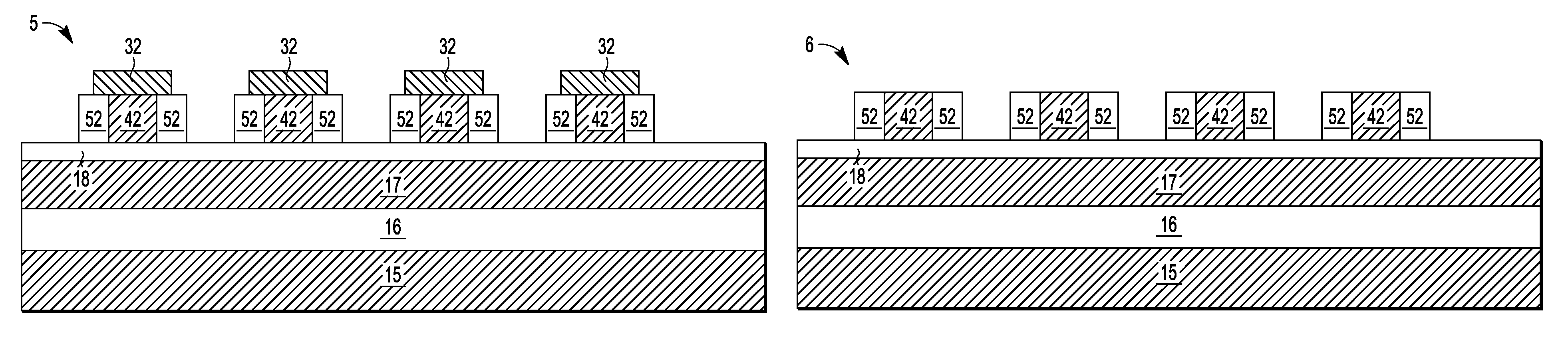
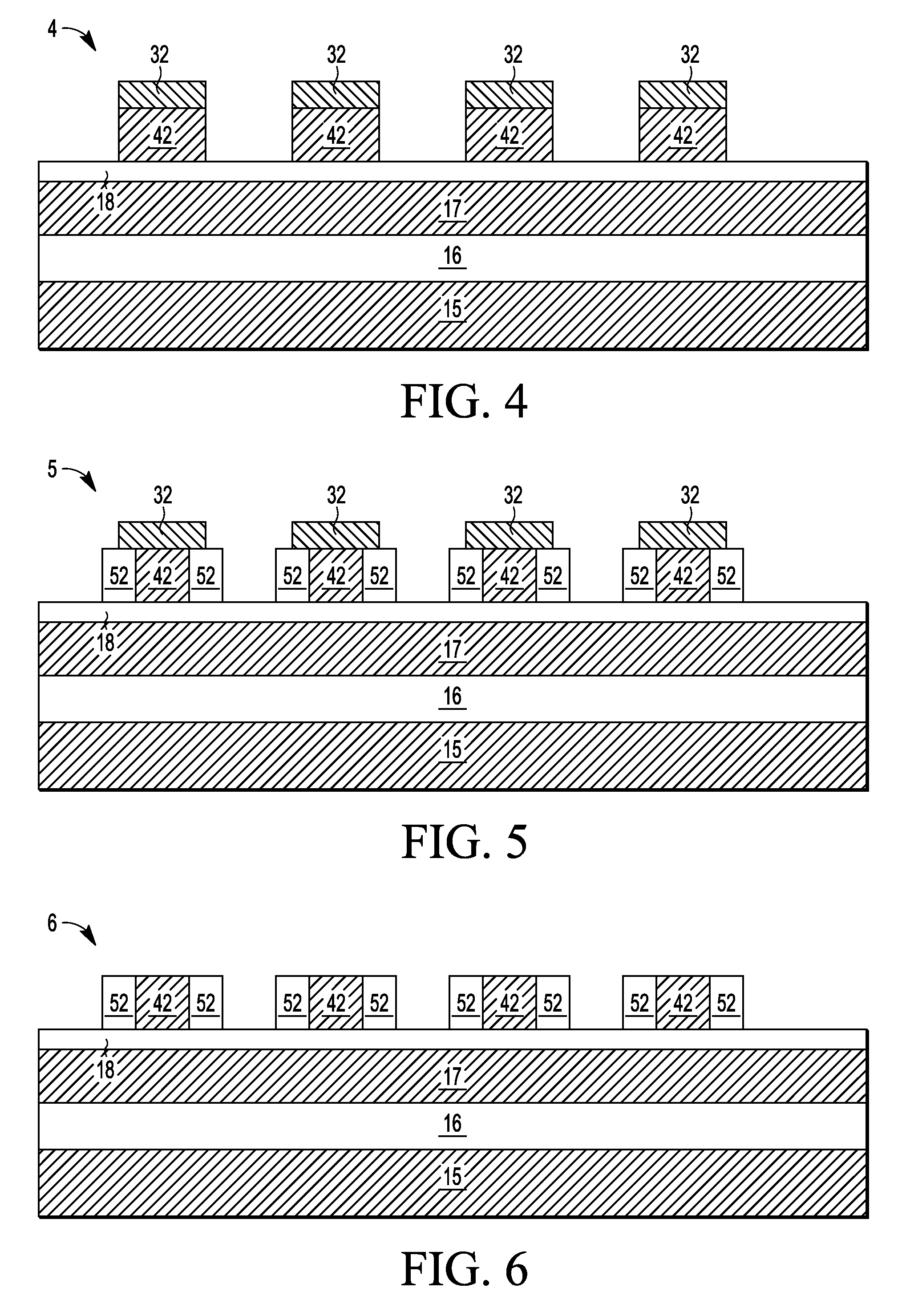
[0020]A method and apparatus are described for fabricating high performance FinFET devices using a double SOI starting substrate where the top SOI semiconductor layer is patterned to form a mandrel of patterned features which are used to pattern the bottom SOI semiconductor layer to form fin structures with tight control of fin pitch and fin thickness. After selectively patterning and trimming the top SOI semiconductor layer to form single crystal dummy structures, the sidewalls of the dummy structures are thermally o...
PUM
| Property | Measurement | Unit |
|---|---|---|
| thickness | aaaaa | aaaaa |
| width | aaaaa | aaaaa |
| thickness | aaaaa | aaaaa |
Abstract
Description
Claims
Application Information