Laser annealing for 3-D chip integration

a technology of laser annealing and 3-d chip, applied in the direction of semiconductor devices, irradiation devices, electric discharge tubes, etc., can solve the problems of fundamental physical limitations, the inability of manufactures to reduce the size of features, and the inability to maintain a proper alignment between separate dies

Inactive Publication Date: 2011-05-24
ULTRATECH INT INC
View PDF14 Cites 7 Cited by
  • Summary
  • Abstract
  • Description
  • Claims
  • Application Information

AI Technical Summary

Problems solved by technology

However, the ability of manufactures to reduce feature size is becoming more expensive and more difficult and beginning to run into fundamental physical limitations.
An issue associated with this technique regards the need to maintain a proper alignment between the separate dies.
However, the alignment issue remains.
Moreover, non-standard connections (e.g., deep vias) are needed to connect the die to the interconnectors of the semiconductor package.
Another issue associated with this technique is that this technique is only directly extendable to two dies, whereas the previously discussed technique may be directly extendable to greater than two dies.

Method used


Image

  • Laser annealing for 3-D chip integration
  • Laser annealing for 3-D chip integration
  • Laser annealing for 3-D chip integration

Examples


Embodiment Construction

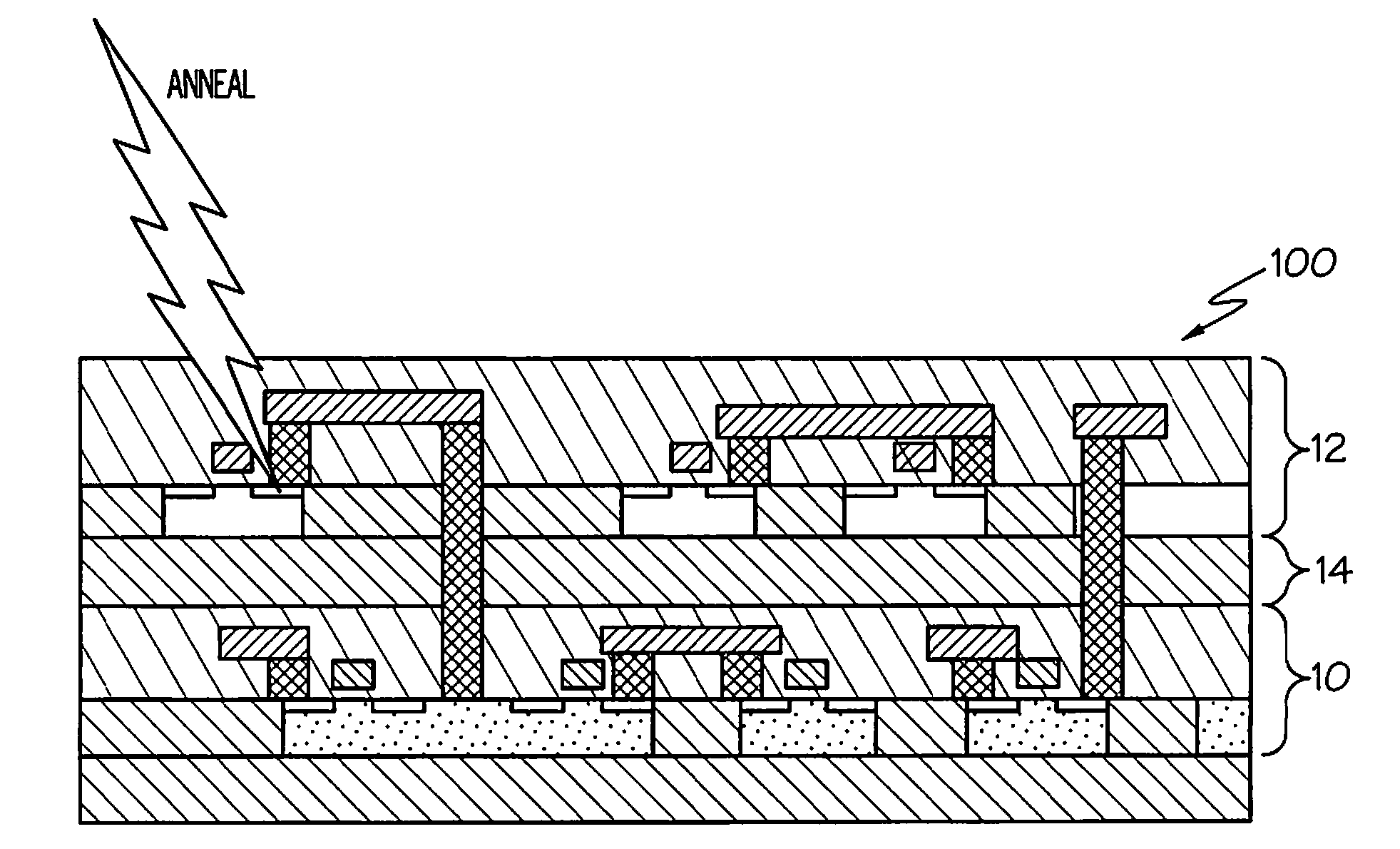
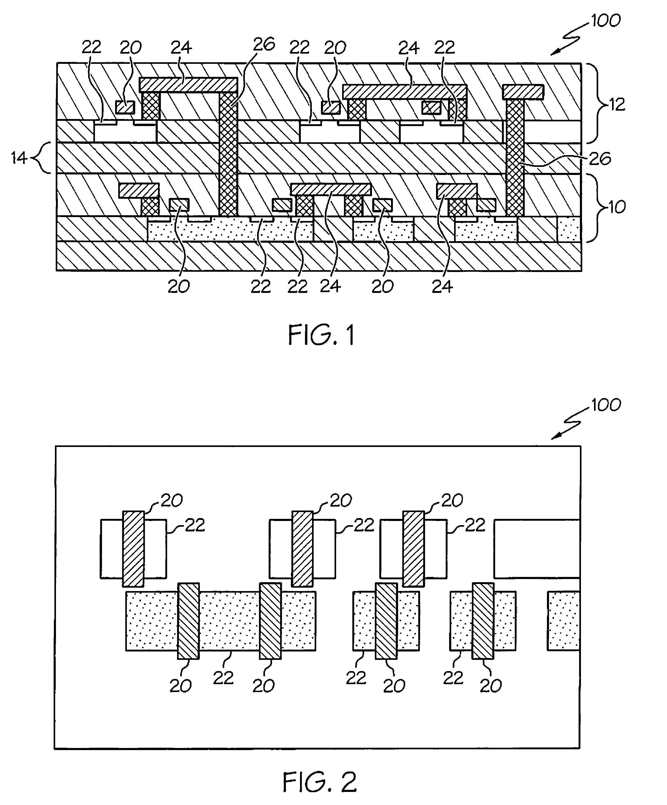
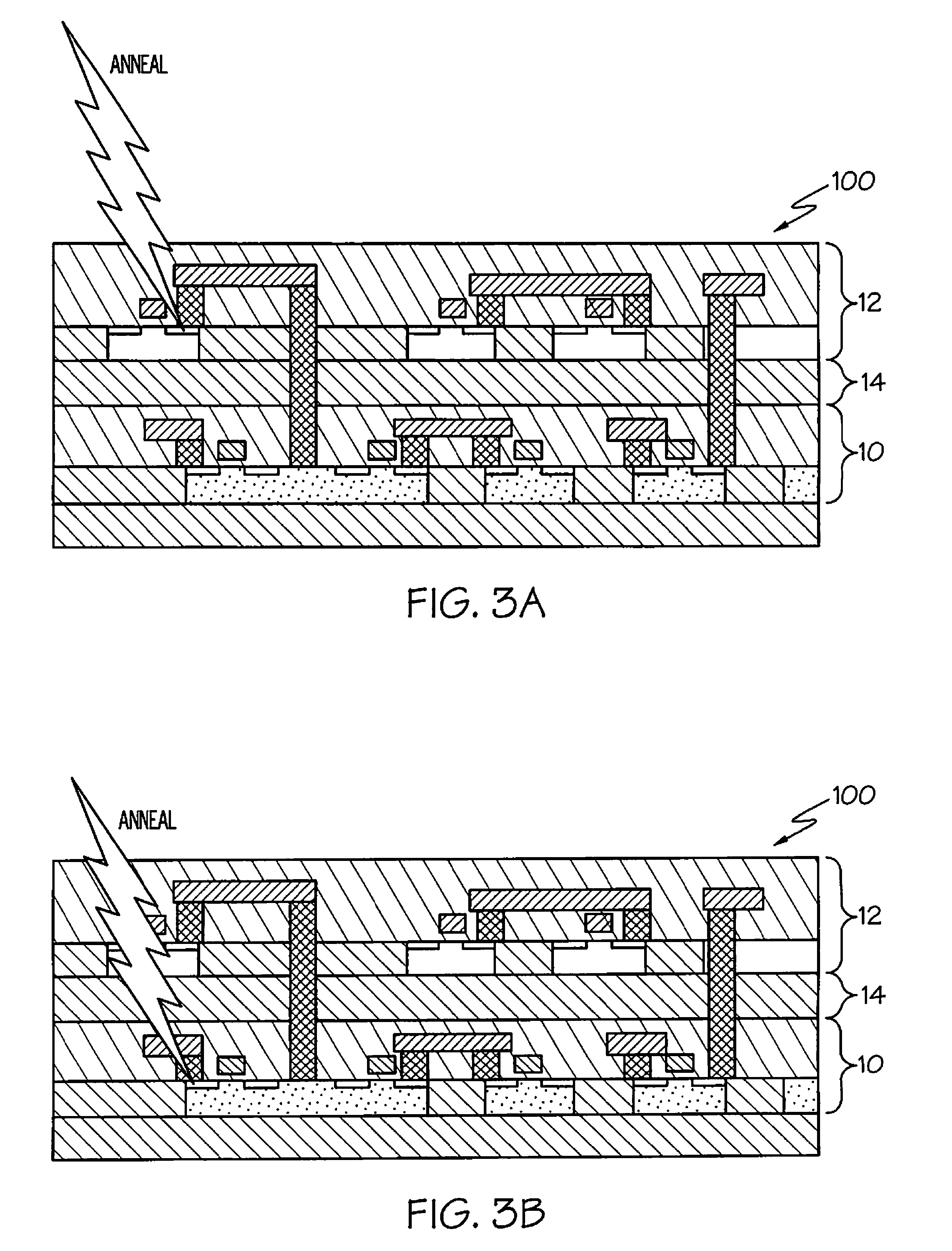
[0024]Referring to FIGS. 1 and 2, a stacked semiconductor structure 100 is illustrated. Although not limited to this specific configuration, the stacked semiconductor structure 100 includes at least two separate stacked layers 10, 12 of active devices (e.g., transistors). Each stacked layer 10, 12 includes a semiconductor material (e.g., silicon, germanium silicon, gallium arsenide) in which semiconductor features such as gates 20, active regions (e.g., source / drain regions 22), and interconnects 24 are formed. Each stacked layer 10, 12 may also include active devices (e.g., transistors) and passive devices (e.g., capacitors, inductors, and resistors) as well as well as other features found in a semiconductor device (e.g., interconnects, doped polysilicon lines, and metal silicide lines). To connect one layer 10 to another layer 12, vias 26 may also be included. An insulation layer 14 (e.g., SiO2) may also be positioned between each stacked layer 10, 12.

[0025]Referring to FIG. 2, th...


PUM


Abstract

A laser annealing method for annealing a stacked semiconductor structure having at least two stacked layers is disclosed. A laser beam is focused on a lower layer of the stacked layers. The laser beam is then scanned to anneal features in the lower layer. The laser beam is then focused on an upper layer of the stacked layers, and the laser beam is scanned to anneal features in the upper layer. The laser has a wavelength of less than one micrometer. The beam size, depth of focus, energy dosage, and scan speed of the laser beam are programmable. Features in the lower layer are offset from features in the upper layer such that these features do not overlap along a plane parallel to a path of the laser beam. Each of the stacked layers includes active devices, such as transistors. Also, the first and second layers may be annealed simultaneously.

Description

BACKGROUND OF THE INVENTION[0001]1. Field of the Invention[0002]The disclosure relates generally to processing of semiconductor devices and, more specifically, to a method of laser annealing sub-surface features in a semiconductor device.[0003]2. Description of the Related Art[0004]To fulfill the ever-increasing demand for computing power, semiconductor chip manufacturers have approached the task of providing more computing power with a single device using various approaches. One of the most commonly used approaches has been to reduce the size of the features in the semiconductor device, which provides the advantages of higher speed, lower power consumption, and a higher density of semiconductor features (e.g., transistors). However, the ability of manufactures to reduce feature size is becoming more expensive and more difficult and beginning to run into fundamental physical limitations.[0005]As a result of these difficulties, many manufacturers are also employing techniques whereby...

Claims


Application Information

Patent Timeline
Patent Type & Authority Patents(United States)
IPC IPC(8): H01L21/44
CPCH01L21/268H01L21/324H01L25/0657H01L24/01H01L27/0688H01L2225/06513H01L2225/06541H01L2924/14H01L2924/00
Inventor CHEN, HOWARD H.HSU, LOUIS C.MOK, LAWRENCE S.SCOTT, J. CAMPBELL
Owner ULTRATECH INT INC
Why Eureka
Try Eureka