

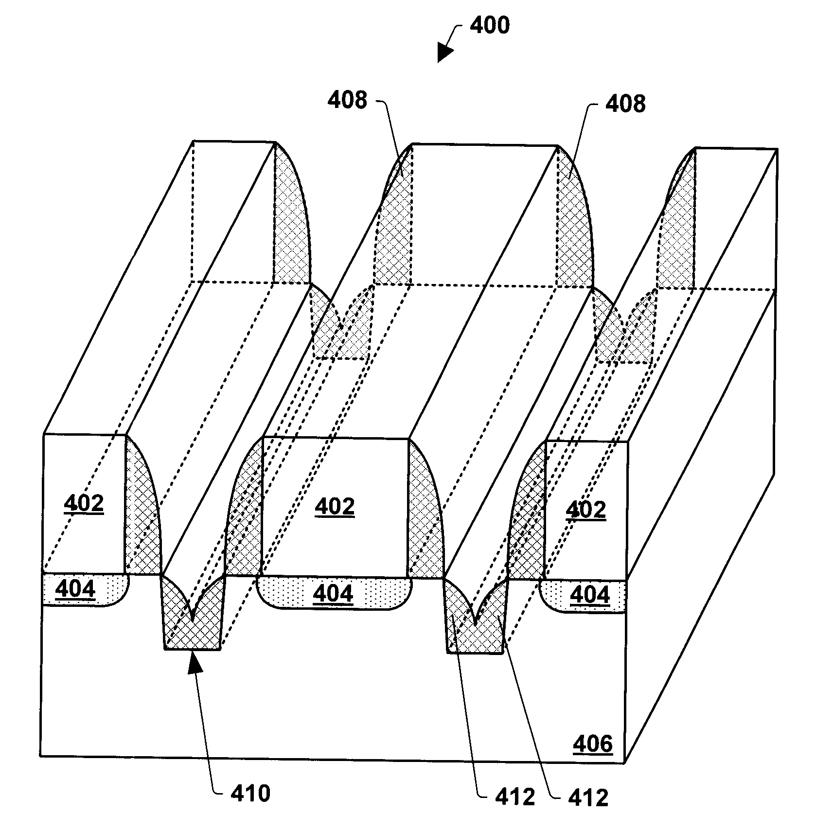
SI trench between bitline HDP for BVDSS improvement
a technology of hdp and trench, applied in the field of memory devices, can solve the problems of increasing the current between the bitlines, increasing so as to improve the bvdss characteristics, prevent and/or mitigate the leakage of bitline to bitline curren
- Summary
- Abstract
- Description
- Claims
- Application Information
AI Technical Summary
Benefits of technology
Problems solved by technology
Method used
Image

Examples
Embodiment Construction
A memory cell, for example, a single bit memory cell or a dual bit memory cell, is programmed by applying a relatively high programming voltage to a control gate and connecting a source to ground and a drain to a predetermined potential above the source. During this process, hot electrons in a core cell channel region near drain inject into the charge storage layer and become trapped since the charge storage layer is electrically isolated from control gate and substrate. As a result of the trapped electrons, the threshold voltage of the cell increases. This change in the threshold voltage (and thereby the channel conductance) of the cell created by the trapped electrons is what causes the cell to be programmed.
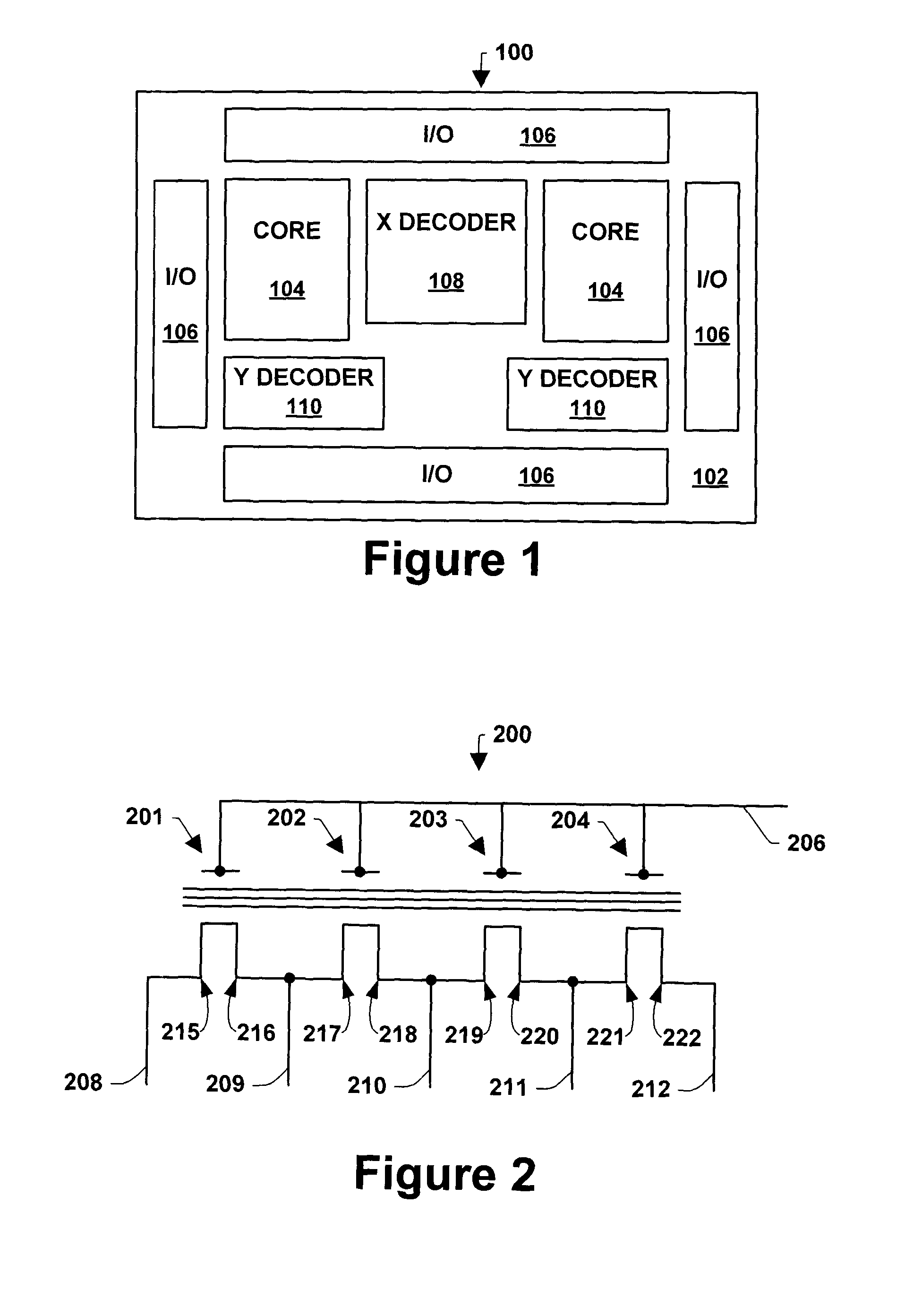
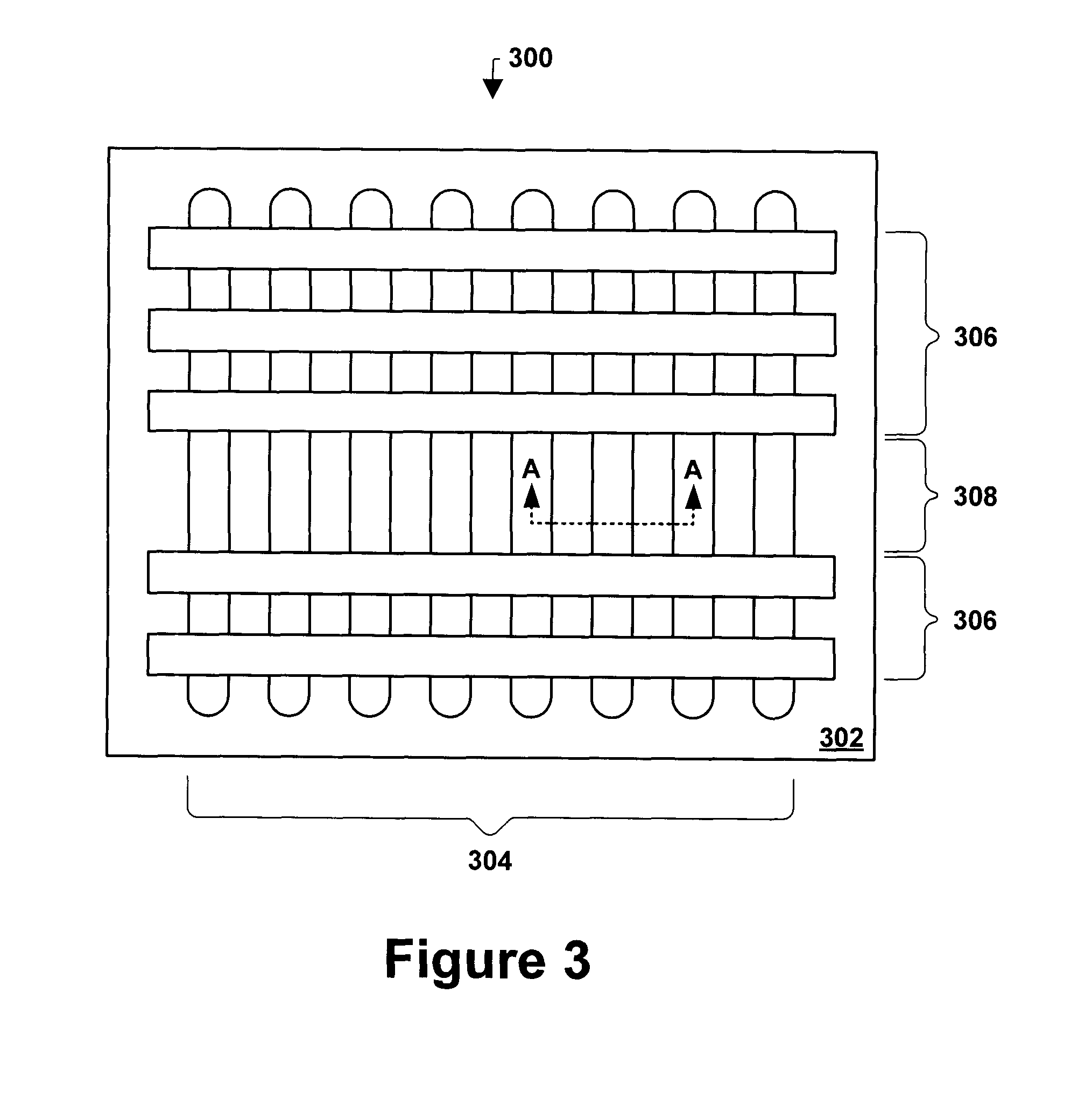
With memory devices shrinking in size, the shorter channel lengths of the smaller devices increasingly exhibit short channel behaviour that affects program operation. As the memory cells shrink, the BVdss also reduces, resulting in increased column leakage current originated f...
PUM
 Abstract
Description
Claims
Application Information