
Method to produce high electron mobility transistors with Boron implanted isolation

a high electron mobility transistor and isolation structure technology, applied in the direction of basic electric elements, electrical apparatus, semiconductor devices, etc., can solve the problems of increasing leakage current, reducing breakdown voltage, and reducing breakdown voltage, so as to prevent the phenomenon of activation, prevent the leakage current, and enhance the electrical isolation of the high electron mobility transistor

Active Publication Date: 2015-09-15
WIN SEMICON
View PDF6 Cites 0 Cited by
  • Summary
  • Abstract
  • Description
  • Claims
  • Application Information

AI Technical Summary

Benefits of technology

The present invention aims to solve two technical problems. Firstly, it aims to improve the electrical isolation of high electron mobility transistors to prevent leakage current. Secondly, it aims to create an ion implantation isolation structure of high electron mobility transistors that can prevent activation and maintain electrical isolation at room temperature.

Problems solved by technology

The disadvantage of the mesa etching is that the mesa sidewall of the device active regions may lead to increasing the leakage current and also reducing the breakdown voltage.
The deeper the mesa sidewall is, the more significant the leakage current is.
Compared with the mesa etching for producing high electron mobility transistors with isolation structure, the ion implantation method saves lots of time and costs of the etching processes and the ion implanted isolation structure may reduce the leakage current problem, and in addition lower the minimum noise figure.
Hence, this will affect the electrical isolation and lead to increasing the leakage current.

Method used


Image

  • Method to produce high electron mobility transistors with Boron implanted isolation
  • Method to produce high electron mobility transistors with Boron implanted isolation
  • Method to produce high electron mobility transistors with Boron implanted isolation

Examples


second embodiment

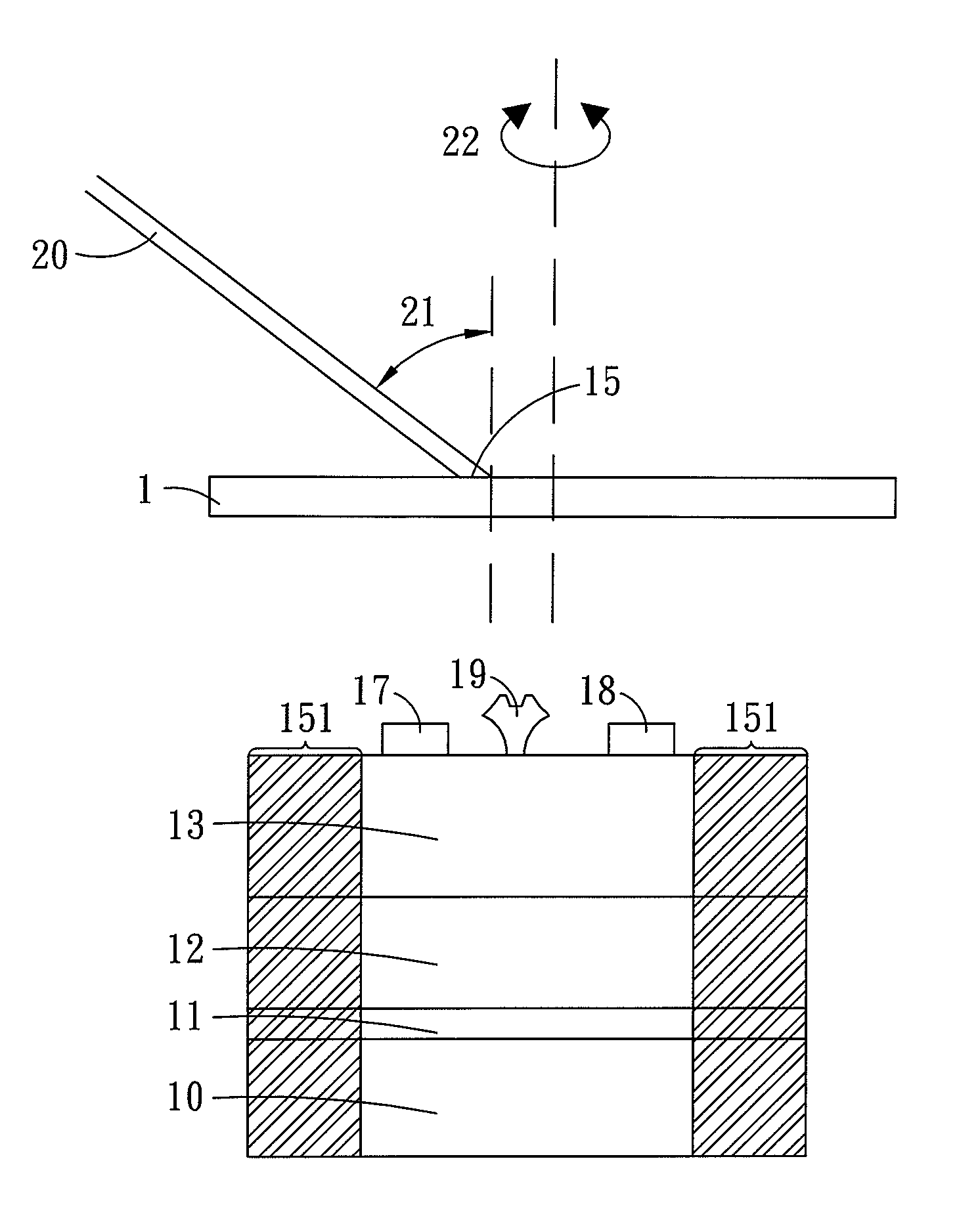
[0034]which is mostly the same as the first embodiment except that executing an ion implantation process plural times includes the following four ion implantation processes: one first ion implantation process, wherein the implantation energy of the Boron ion beam 20 is between 10 KeV and 50 KeV, and the Boron ions of the Boron ion beam 20 are at a dose of 1011 / cm−3 to 1013 / cm−3; two second ion implantation processes, wherein the implantation energy of the Boron ion beam 20 is between 50 KeV and 200 KeV, and the Boron ions of the Boron ion beam 20 are at a dose of 1012 / cm−3 to 1013 / cm−3; and one third ion implantation process, wherein the implantation energy of the Boron ion beam 20 is between 200 KeV and 300 KeV, and the Boron ions of the Boron ion beam 20 are at a dose of 1012 / cm−3 to 1013 / cm−3.

[0035]In the second embodiment, the substrate 10 is made of SiC; the nucleation layer 11 is made of AlN; the buffer layer 12 is made of GaN; and the barrier layer 13 is made of AlGaN; the in...

third embodiment

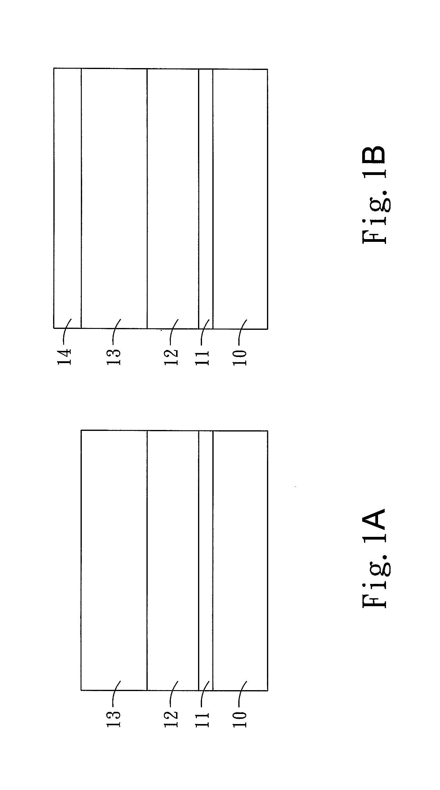
[0036]please refer to FIG. 2A˜2H, which show the process flow diagram of an embodiment of the present invention. Forming the structure as shown in FIG. 2A by the following four steps: forming a nucleation layer 11 on a substrate 10; forming a buffer layer 12 on the nucleation layer 11; forming a barrier layer 13 on the buffer layer 12 and forming a cap layer 16 on the barrier layer 13. After these four steps, the structure, shown in FIG. 2A, with the substrate 10, the nucleation layer 11, the buffer layer 12, the barrier layer 13 and the cap layer 16 is formed.

[0037]The substrate 10 is made of SiC, Si, Diamond, Sapphire or GaN; the nucleation layer 11 is made of AlN; the buffer layer 12 is made of GaN, AlGaN or AlN; the barrier layer 13 is made of AlGaN or InAlN; and the cap layer is made of GaN.

[0038]Please refer to FIG. 2B, which shows the step: coating a photoresist layer 14 on the cap layer 16.

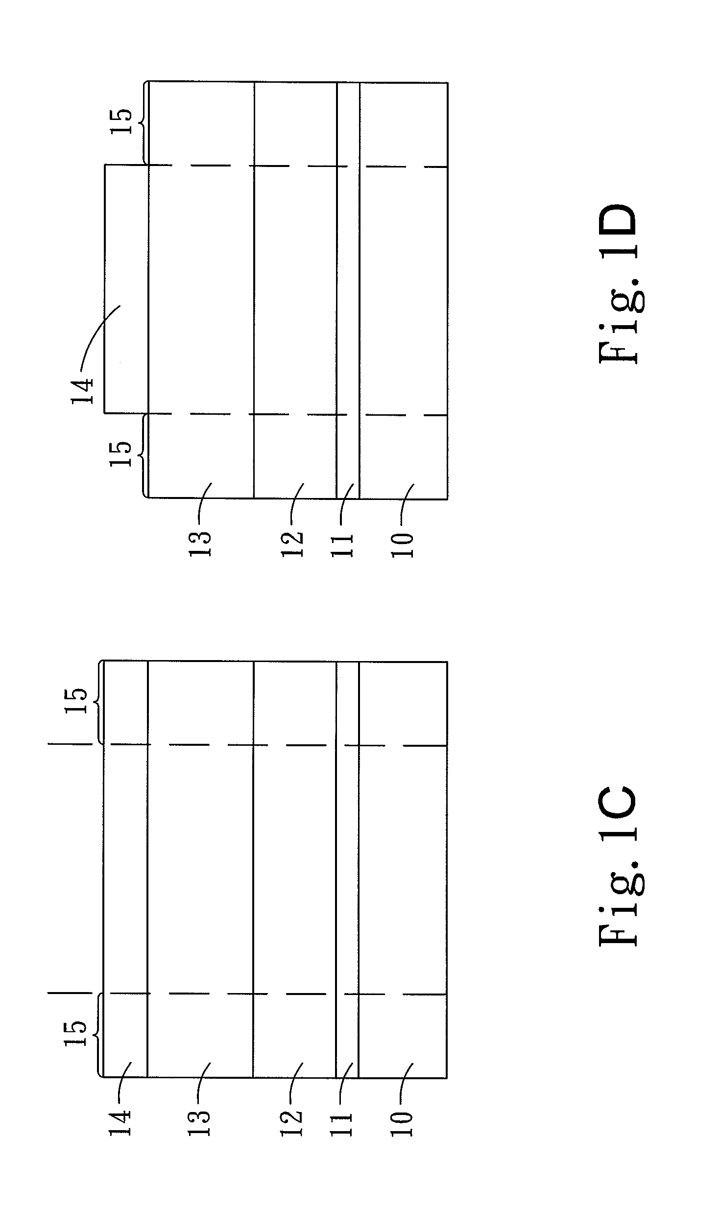
[0039]Please refer to FIG. 2C, which shows the step: photomasking at least one isolati...

fourth embodiment

[0050]which is mostly the same as the third embodiment except that executing an ion implantation process plural times includes the following four ion implantation processes: one first ion implantation process, wherein the implantation energy of the Boron ion beam 20 is between 10 KeV and 50 KeV, and the Boron ions of the Boron ion beam 20 are at a dose of 1011 / cm−3 to 1013 / cm−3; two second ion implantation processes, wherein the implantation energy of the Boron ion beam 20 is between 50 KeV and 200 KeV, and the Boron ions of the Boron ion beam 20 are at a dose of 1012 / cm−3 to 1013 / cm−3; and one third ion implantation process, wherein the implantation energy of the Boron ion beam 20 is between 200 KeV and 300 KeV, and the Boron ions of the Boron ion beam 20 are at a dose of 1012 / cm−3 to 1013 / cm−3.

[0051]In the fourth embodiment, the substrate 10 is made of SiC; the nucleation layer 11 is made of AlN; the buffer layer 12 is made of GaN; and the barrier layer 13 is made of AlGaN; the ca...


PUM


Abstract

A method to produce high electron mobility transistors with Boron implanted isolation comprises the following steps: on a substrate forming in sequence a nucleation layer, a buffer layer, a barrier layer and a cap layer; coating a photoresist layer on the cap layer; photomasking and by exposure eliminating the photoresist layer of at least one isolation region; executing plural times an ion implantation process including: adjusting an incident angle of a Boron ion beam with respect to the substrate, and implanting the Boron ion beam into the cap layer, the barrier layer, the buffer layer, the nucleation layer and the substrate within the at least one isolation region so as to form an isolation structure while rotating the substrate by a rotation angle; eliminating the rest of the photoresist layer by exposure; and forming a source, a drain and a gate on the cap layer.

Description

FIELD OF THE INVENTION[0001]The present invention relates to a method to produce high electron mobility transistors with Boron implanted isolation structure, with enhanced electrical isolation and reduced the leakage phenomenon. The high electron mobility transistors with Boron implanted isolation structure may be produced under room temperature that may prevent the phenomenon of activation so as to preserve the electrical isolation.BACKGROUND OF THE INVENTION[0002]There are mainly two ways for producing high electron mobility transistors with isolation structure in conventional technique. One is the mesa etching, by etching the device non-active regions to fabricate the isolation structure; the other is ion implantation, by implanting ion beam into the device non-active regions to produce the isolation structure. The disadvantage of the mesa etching is that the mesa sidewall of the device active regions may lead to increasing the leakage current and also reducing the breakdown volt...

Claims


Application Information

Patent Timeline
IPC IPC(8): H01L21/338H01L29/66H01L21/761
CPCH01L29/66431H01L21/761H01L21/26586H01L29/66462H01L29/2003H01L21/2654H01L29/7786
Inventor WOHLMUTH, WALTER TONYWANG, WEI-CHOUDU, JHIH-HANHSIEH, YAO-CHUNGHUANG, SHIH HUI
Owner WIN SEMICON
Learn More