Semiconductor device and formation method therefor

A technology of semiconductors and devices, applied in the field of semiconductor manufacturing, to achieve the effect of improving the electrical isolation effect and optimizing the electrical performance

Active Publication Date: 2016-02-17
SEMICON MFG INT (SHANGHAI) CORP
View PDF7 Cites 12 Cited by
  • Summary
  • Abstract
  • Description
  • Claims
  • Application Information

AI Technical Summary

Problems solved by technology

[0006] The problem solved by the present invention is to prevent the dopant ions in the first well region from diffusing into the isolation structure, and to prevent the dopant ions in the second well region from diffusing into the isolation structure, preventing the first well region and the second well region from The concentration of doping ions is reduced to ensure the electrical isolation effect of semiconductor devices

Method used


Image

  • Semiconductor device and formation method therefor
  • Semiconductor device and formation method therefor
  • Semiconductor device and formation method therefor

Examples


Embodiment Construction

[0034] It can be seen from the background art that the electrical performance of semiconductor devices formed in the prior art needs to be improved.

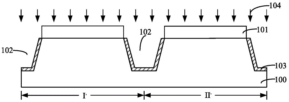
[0035] It has been found through research that as the size of semiconductor devices continues to shrink, the problems caused by the diffusion of dopant ions in the well region to the isolation structure become more and more serious, resulting in changes in the threshold voltage of semiconductor devices, and the gap between the well region and the heavily doped region The leakage current problem of the semiconductor device becomes serious, and the electrical isolation effect of the semiconductor device is very poor.

[0036] In order to reduce the diffusion of dopant ions in the well region into the isolation structure, a method for forming a semiconductor device is proposed:

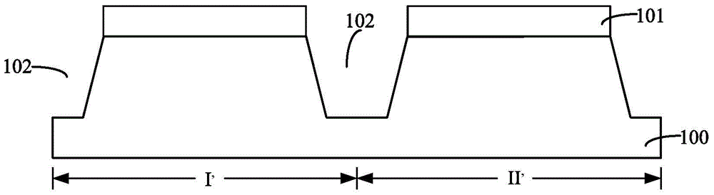
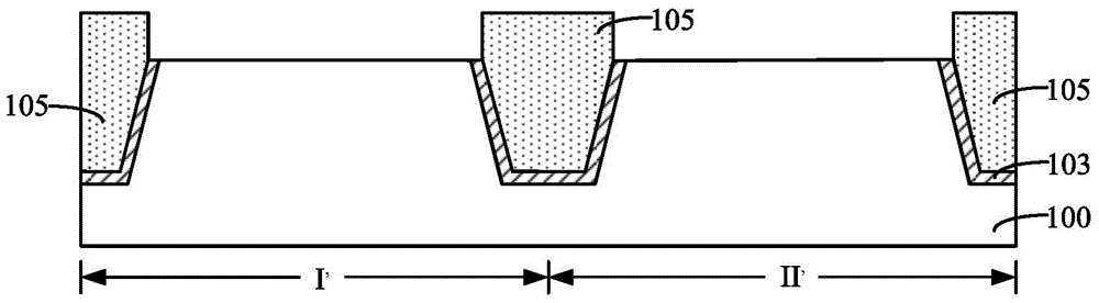
[0037] Please refer to figure 1 , provide a substrate 100, the substrate 100 includes a first region I' and a second region II', a patterned mask layer ...


PUM


Abstract

A semiconductor device and a formation method therefor are disclosed. The formation method for the semiconductor device comprises the steps of providing a substrate including a first region and a second region; forming a groove including a first part and a second part in the substrate; forming a first barrier layer at the bottom of the first part and the surface of the side wall of the groove, wherein the first barrier layer captures lattice vacancy defects or interstitial atom defects in the substrate; forming a second barrier layer at the bottom of the second part and the surface of the side wall of the groove, wherein the second barrier layer captures lattice vacancy defects or interstitial atom defects in the substrate, and defect types captured by the first barrier layer and the second barrier layer are different; forming dielectric layers for filling the grooves; forming a first well region in the first region substrate; forming a second well region in the second region substrate, wherein the doping types of the second well region and the first well region are opposite. According to the semiconductor device and the formation method therefor, the diffusion of the doping ions in the first well region and the second well region can be effectively prevented to endow the semiconductor device with a good electrical isolation performance.

Description

technical field [0001] The invention relates to the technology in the field of semiconductor manufacturing, in particular to a semiconductor device and a forming method thereof. Background technique [0002] In semiconductor manufacturing technology, in order to electrically isolate different semiconductor devices manufactured on the semiconductor substrate, an isolation structure is usually formed between different semiconductor devices on the semiconductor substrate. [0003] Methods for forming the isolation structure include: a local oxidation isolation (LOCOS) method and a shallow trench isolation (STI: Shallow Trench Isolation) method. Compared with other isolation methods, the shallow trench isolation method has many advantages, mainly including: the shallow trench isolation method can obtain a narrower semiconductor device isolation width, reduce the area occupied by the semiconductor substrate and increase the active region width of the device, and then Improve the...

Claims


Application Information

Patent Timeline
Patent Type & Authority Applications(China)
IPC IPC(8): H01L21/762H01L29/06
Inventor 赵猛
Owner SEMICON MFG INT (SHANGHAI) CORP
Why Eureka
Try Eureka