

Radiation sensors and single-event-effects suppression devices
a technology of radiation sensor and suppression device, which is applied in the direction of information storage, static storage, digital storage, etc., can solve the problems of high cost of hardened circuit, insufficient protection, and inability to provide acceptable levels of protection
- Summary
- Abstract
- Description
- Claims
- Application Information
AI Technical Summary
Problems solved by technology
Method used
Image

Examples
first embodiment
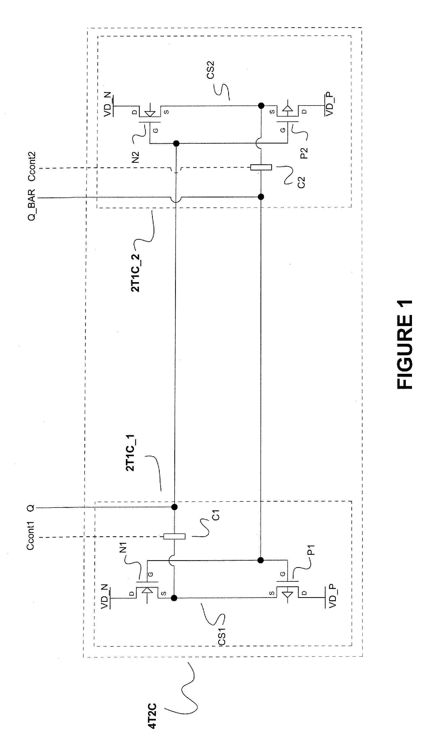
FIG. 1
[0014]FIG. 1 is a transistor level circuit diagram showing a Four-Transistor Two-Capacitor Radiation Single-Event-Effects Suppression Device 4T2C according to a first embodiment of this invention.
[0015]The Four-Transistor Two-Capacitor Radiation Single-Event-Effects Suppression Device 4T2C includes a first Two-Transistor One-Capacitor Radiation Single-Event-Effects Suppression Device 2T1C_1, a second Two-Transistor One-Capacitor Radiation Single-Event-Effects Suppression Device 2T1C_2, a first optional capacitor device control line Cont1, a second optional capacitor device control line Cont2, a first Bi-Directional Input / Output terminal Q, and a second Bi-Directional Input / Output terminal Q_BAR.
[0016]The first Two-Transistor One-Capacitor Radiation Single-Event-Effects Suppression Device 2T1C_1 includes an N-type transistor device N1, a P-type transistor device P1, a capacitor device C1, a Common Source Terminal CS1, a high power supply node VD_N, and a low power supply node V...
second embodiment
FIG. 2
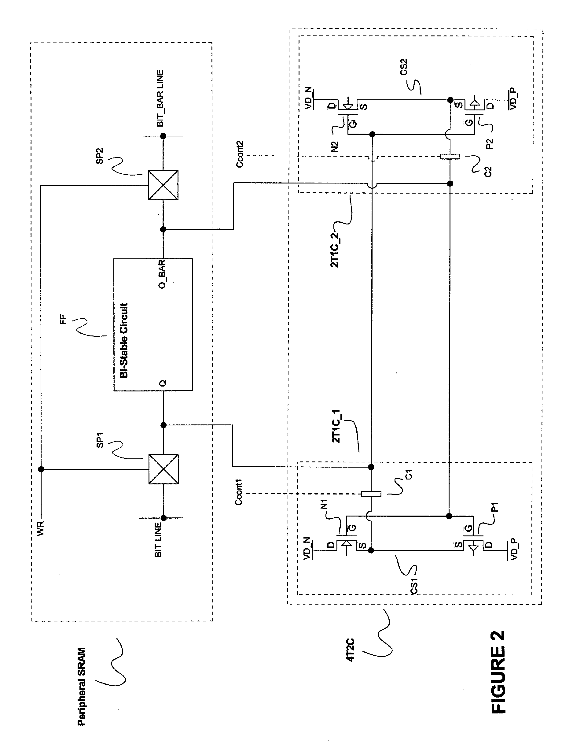
[0072]FIG. 2 is a block diagram of a peripheral bi-stable circuit in an SRAM circuit configuration Peripheral SRAM and a transistor level circuit diagram showing a Four-Transistor Two-Capacitor Radiation Single-Event-Effects Suppression Device 4T2C according to a second embodiment of this invention.
[0073]The Peripheral SRAM circuit includes a Bi-Stable Circuit FF, a first Series-Pass-Element SP1, a second Series-Pass-Element SP2, a Write / Read control line WR, a first Bi-Directional data line BIT LINE, and a second Bi-Directional data line BIT_BAR LINE. The Bi-Stable Circuit FF having a first Bi-Directional Input / Output terminal Q and a second Bi-Directional Input / Output terminal Q_BAR. The first Series-Pass-Element SP1 having an input control terminal coupled to WR, a first Bi-Directional Input / Output terminal coupled to Bi-Directional data line BIT LINE, and a second Bi-Directional Input / Output terminal coupled to the Bi-Directional Input / Output terminal Q. The Second Series-...
third embodiment
FIG. 3
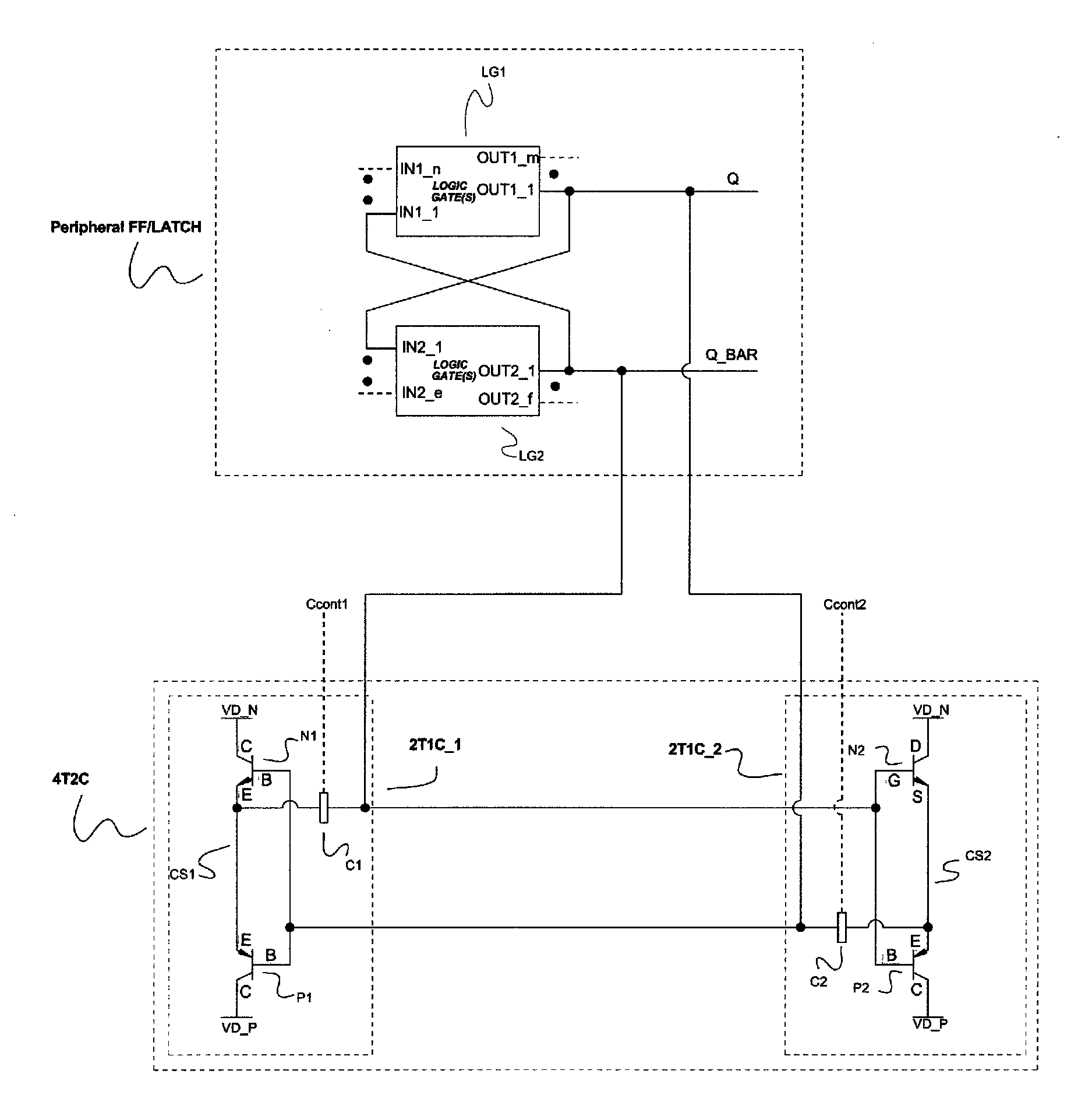
[0090]FIG. 3 is a block diagram of a peripheral bi-stable circuit in a Flip-Flop or Latch circuit configuration Peripheral FF / LATCH and a transistor level circuit diagram showing a Four-Transistor Two-Capacitor Radiation Single-Event-Effects Suppression Device 4T2C according to a third embodiment of this invention.
[0091]The peripheral FF / LATCH circuit includes a first LOGIC GATE(S) LG1, a second LOGIC GATE(S) LG2, a first output terminal Q, and a second output terminal Q_BAR. The first LOGIC GATE(S) LG1 having a first input IN1_1 coupled to the output terminal Q_BAR, zero (0) to “n” additional optional inputs, an output OUT1_1 coupled to the output terminal Q, and zero (0) to “m” additional optional outputs. The second LOGIC GATE(S) LG2 having a first input IN2_1 coupled to the output terminal Q, zero (0) to “e” additional optional inputs, an output OUT2_1 coupled to the output terminal Q_BAR, and zero (0) to “f” additional optional outputs.
[0092]The Four-Transistor Two-Capaci...
PUM
 Abstract
Description
Claims
Application Information