Low-cost substrates having high-resistivity properties and methods for their manufacture

a technology of resistivity properties and low-cost substrates, which is applied in the direction of electrical equipment, semiconductor devices, radio frequency controlled devices, etc., can solve the problems of high cost, high cost, and often higher cost of hr supports, and achieve high resistivity properties and reduce the thickness of the donor substra

Active Publication Date: 2011-07-12
SOITEC SA
View PDF60 Cites 6 Cited by
  • Summary
  • Abstract
  • Description
  • Claims
  • Application Information

AI Technical Summary

Benefits of technology

[0006]The present invention provides high-resistivity “HR” substrates—that is substrates structured so that devices fabricated in a top layer thereof have properties similar to the same devices fabricated in a standard high resistivity substrate—that are simpler to manufacture and of lower cost than known HR substrates. HR substrates of this invention have applications in microelectronics, optoelectronics, photovoltaics, micro-electro mechanical devices, and particularly in devices that operate at high frequency typically over 100 Mhz, such as radio frequency devices that can be found in telecommunication or radio detection applications.
[0007]In general, the invention replaces known, higher-cost HR substrates with lower-cost, HR substrates comprising a top layer and a support. Instead of relying on high-resistivity of the support to provide high-resistivity of the final substrate, the invention provides high-resistivity of the final substrate by means of a support with a surface layer of a lower-cost, high-resistivity semiconductor material. Accordingly, the support can have standard resistivity, and optionally lower quality, and thus can be of lower cost. The invention also provides low-cost methods for manufacturing HR substrates.

Problems solved by technology

Although known HR substrates are suitable for devices with improved performance because they provide reduced signal loss in the support or improved signal to noise ratio due to reduced crosstalk, they suffer from a major drawback: their cost can be high.
High cost is a particular concern when substrates will be used for fabrication of devices to be integrated into price sensitive products, such as consumer products telecom markets
The higher cost of HR supports often arises because their manufacture requires additional steps.

Method used


Image

  • Low-cost substrates having high-resistivity properties and methods for their manufacture
  • Low-cost substrates having high-resistivity properties and methods for their manufacture
  • Low-cost substrates having high-resistivity properties and methods for their manufacture

Examples


Embodiment Construction

[0015]The preferred embodiments and particular examples described herein should be seen as examples of the scope of the invention, but not as limiting the present invention. The scope of the present invention should be determined with reference to the claims.

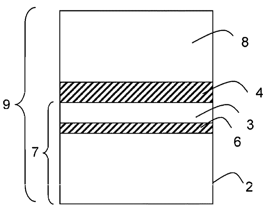
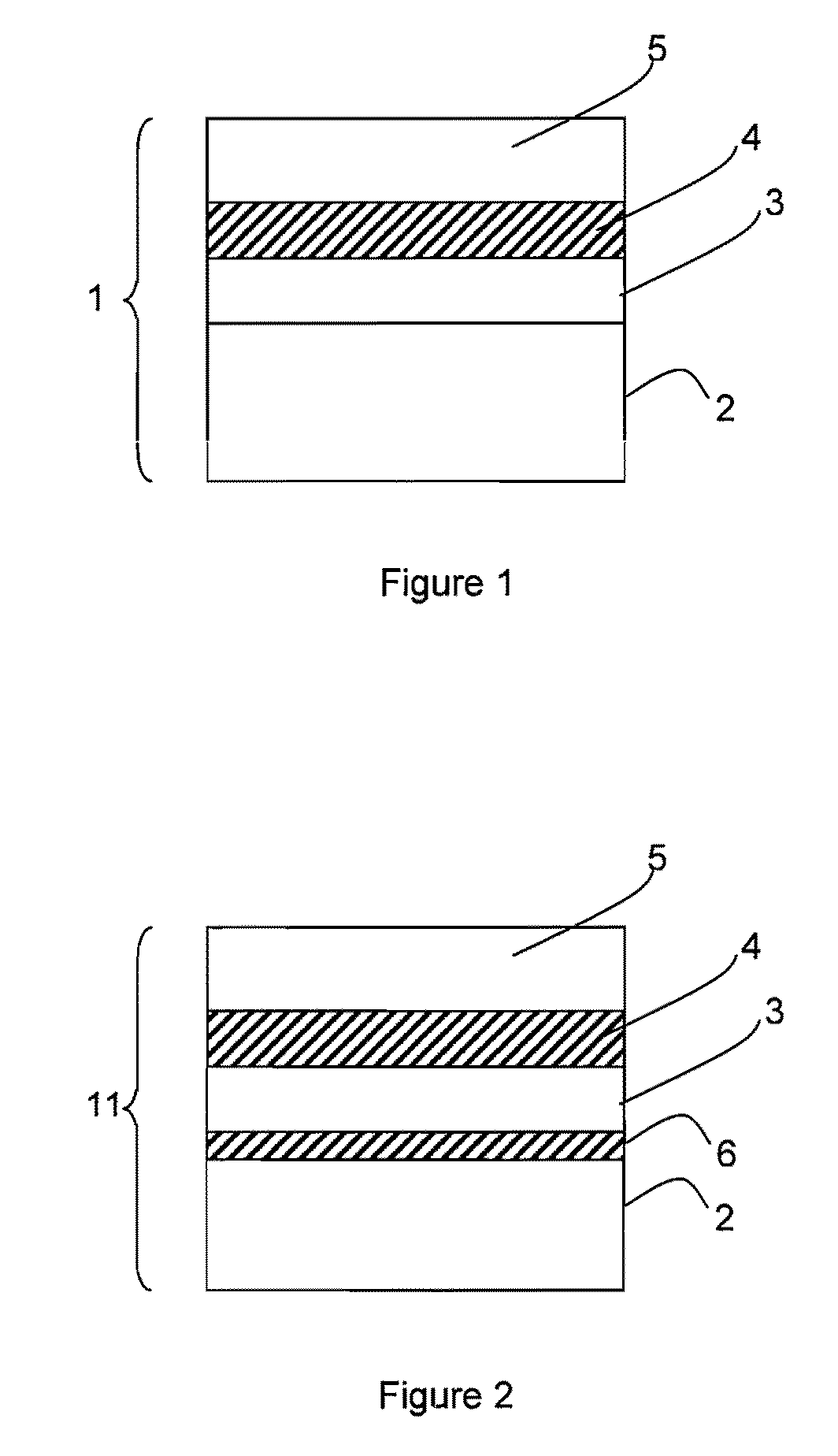
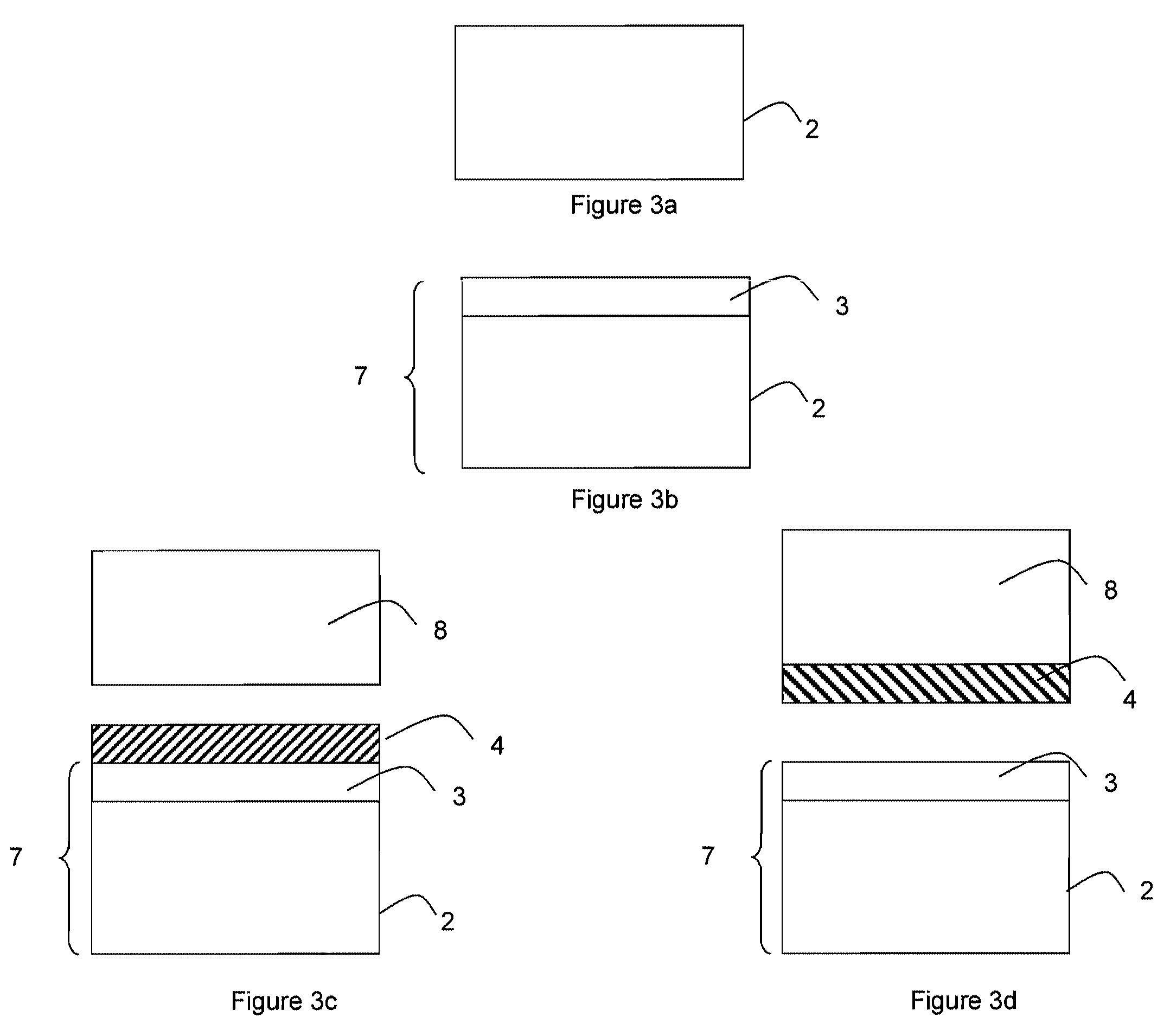
[0016]FIG. 1 illustrates embodiments according to the invention of substrates 1 structured so that devices fabricated in a top layer thereof have properties similar to the same devices fabricated in a standard high resistivity substrate. These substrates of the invention are also more simply referred to herein as “HR substrates”. The substrate 1 can have a diameter depending on its final application of, e.g., 300 mm, 200 mm, or other diameters.

[0017]Substrate 1 comprises top layer 5, in which or on which devices are ultimately formed. In some cases, devices, e.g., known CMOS devices, can be formed according to known techniques directly on and in top layer 5. In other cases, e.g., gallium nitride HEMT devices, further layers (not...


PUM


Abstract

In one embodiment, the invention provides substrates that are structured so that devices fabricated in a top layer thereof have properties similar to the same devices fabricated in a standard high resistivity substrate. Substrates of the invention include a support having a standard resistivity, a semiconductor layer arranged on the support substrate having a high-resistivity, preferably greater than about 1000 Ohms-cm, an insulating layer arranged on the high-resistivity layer, and a top layer arranged on the insulating layer. The invention also provides methods for manufacturing such substrates.

Description

[0001]This application claims the benefit of application No. 61 / 093,887 filed Sep. 3, 2008, the entire content of which is expressly incorporated herein by reference thereto.BACKGROUND OF THE INVENTION[0002]The present invention relates to substrates structured so that devices fabricated in a top layer thereof have properties similar to the same devices fabricated in a standard high resistivity substrate, and to methods of manufacturing such substrates.BACKGROUND OF THE INVENTION[0003]Examples of known substrates with high electrical resistivity “HR” substrates are disclosed in documents US 2006 / 0166451 and US 2007 / 0032040. Such known substrates generally comprise a top layer in which or on which high frequency devices will be formed, an insulating layer below the top layer and a high-resistivity support. In some instances, additional layers could be inserted between the insulating layer and the support to further improve the high electrical resistivity properties of the substrate.[...

Claims


Application Information

Patent Timeline
Patent Type & Authority Patents(United States)
IPC IPC(8): H01L29/02
CPCH01L21/76251
Inventor NGUYEN, BICH-YENMAZURE, CARLOS
Owner SOITEC SA
Why Eureka
Try Eureka