Optical transmitter with a shunt driving configuration and a load transistor operated in common gate mode

a technology of optical transmitter and load transistor, which is applied in the direction of semiconductor lasers, electrical equipment, laser details, etc., can solve the problems of substantially short circuit of gate bias and abnormal power supply, and achieve the effect of suppressing driving signal infection, small input, and large output impedan

Active Publication Date: 2011-07-12
SUMITOMO ELECTRIC IND LTD
View PDF9 Cites 0 Cited by
  • Summary
  • Abstract
  • Description
  • Claims
  • Application Information

AI Technical Summary

Benefits of technology

[0007]The transistor operated in the common gate mode has large output impedance viewed from the drain thereof, while, small input impedance viewed from the source. The drain of the load transistor connects to the LD and the switching transistor, and the source connects to the power supply. Therefore, in the circuit configuration of the present invention, high frequency components contained in the driving signal is hard to appear in the source of the load transistor, which suppresses the infection of the driving signal to the power supply and, accordingly, the degradation in the optical output from the transmitter.
[0008]The transmitter of the present invention may include a bias generator within the CAN package to further stabilize the bias applied to the gate of the load transistor, which enhances the common gate operation of the load transistor. Moreover, the transmitter may further provide a switch and a detector. The switch is interposed between the gate of the load transistor and the bias generator, and the detector detects the abnormality of the power supply. When an abnormality is detected, the switch between the gate and the bias generator is turned off, which forces the gate bias to be substantially short-circuited to the source of the load transistor. As a result, the current to be supplied to the LD is cut to prevent the LD from the breakdown. A breaking of the wire or a breakdown of devices within the APC feedback loop may cause the abnormality of the power supply. According to the present invention, even such abnormality may occur, the LD can be reliably protected.

Problems solved by technology

When an abnormality is detected, the switch between the gate and the bias generator is turned off, which forces the gate bias to be substantially short-circuited to the source of the load transistor.
A breaking of the wire or a breakdown of devices within the APC feedback loop may cause the abnormality of the power supply.

Method used


Image

  • Optical transmitter with a shunt driving configuration and a load transistor operated in common gate mode
  • Optical transmitter with a shunt driving configuration and a load transistor operated in common gate mode
  • Optical transmitter with a shunt driving configuration and a load transistor operated in common gate mode

Examples


first embodiment

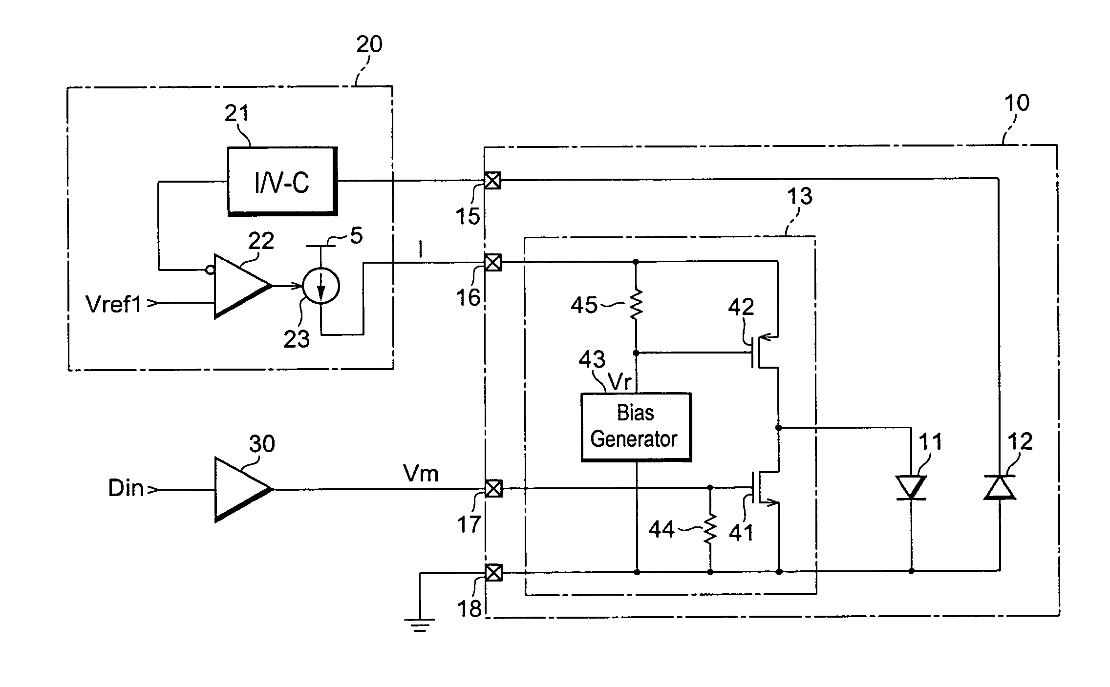
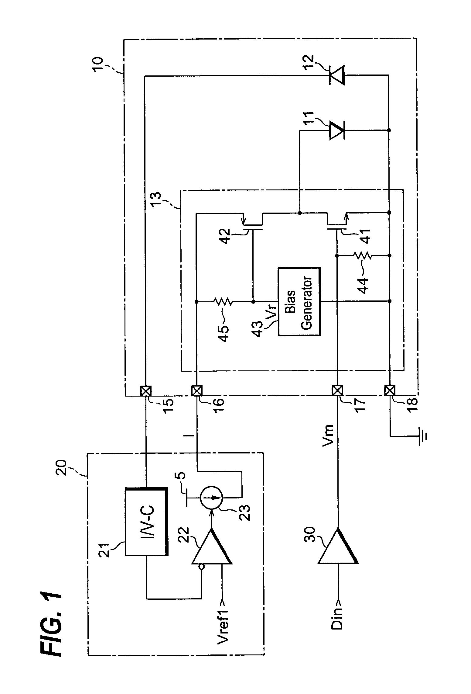
[0015]FIG. 1 is a circuit diagram of an optical transmitter 10 according to the first embodiment of the present invention. FIG. 1 illustrates, in addition to the optical transmitter 10, an auto-power control (hereafter denoted as APC) block 20 and a signal driver 30. The optical transmitter 10 includes a semiconductor laser diode (hereafter denoted as LD) 11, a photodiode (hereafter denoted as PD) 12, and a driver 13. The optical transmitter further provides a monitoring terminal 15, a power supply terminal 16, a signal terminal 17 and a ground terminal 18.

[0016]The LD 11 is connected to a current source 23 within the APC block 20 through the power supply terminal 16 to be provided with a driving current from the current source 23. The LD 12, by providing the driving current, is able to emit light. The PD 12 monitors the optical power emitted from the LD 11. The PD 12 generates a photocurrent substantially proportional to the optical power emitted from the LD 11. The optical transmi...

second embodiment

[0031]FIG. 3 is a block diagram of an optical transmitter 10A according to the second embodiment of the present invention. This transmitter 10A includes, in addition to elements shown in FIG. 1, an inductor 46 inserted between the drain of the second transistor 42 and the drain of the first transistor 41.

[0032]The second transistor 42 inherently provides the parasitic capacitance between the drain and the source thereof, which degrades the isolation between the drain and the source for high frequency components of the driving signal Vm. The impedance of the inductor 46 between the drains of the transistor, 41 and 42, increases as the frequency becomes high, which compensates the degradation in the isolation by the transistor 42 at quite high frequencies. In addition, the inductor 46 may isolate the first transistor 41 from the parasitic capacitance between the drain and the source of the second transistor. Thus, the embodiment shown in FIG. 3 may suppress the high frequency componen...

third embodiment

[0033]The power detector 47, which is connected to the power supply terminal 16 and the source of the transistor 42, is configured to detect the level V1 at the power supply terminal 16, to compare the level V1 with a reference VTh1, and to control the switch 46 in accordance with the comparison. The detector 47 turns off the switch 46 when the level V1 becomes greater than VTh1, while, it turns on in other cases between the level V1 and the reference Vref2. Thus, the bias of the transistor 42, namely, the voltage difference between the source and the gate of the transistor 42 occasionally becomes substantially zero.

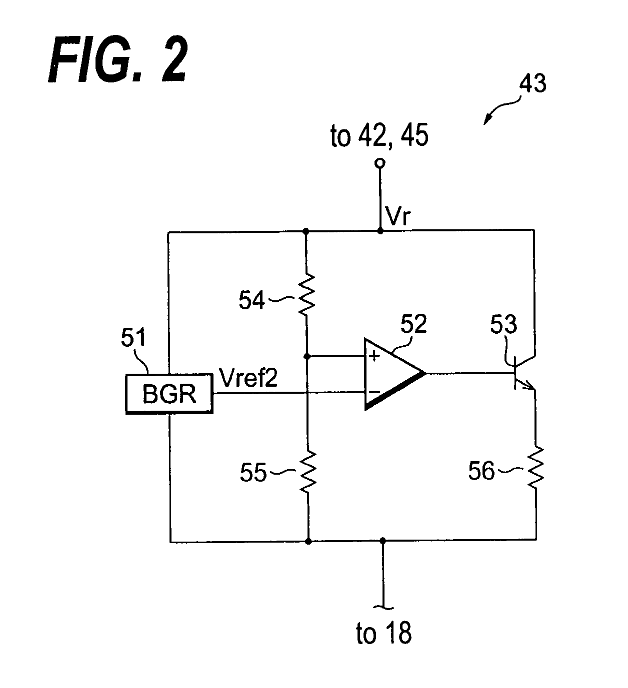
[0034]The bias generator 43 in the output Vr thereof is provided to the gate of the transistor 42 through the switch 46. When the switch 46 is turns on, the gate of the transistor 42 may be stabilized in the level Vr, which is the same condition with the case in the first and the second embodiments.

[0035]When the level V1 at the power supply terminal 16 becomes large due...


PUM


Abstract

The invention provides an optical transmitter that prevents the high frequency components in the driving signal from leaking to the external power supply in a wider frequency range. The transmitter provides a shun driving configuration with a switching transistor connected in parallel to the laser diode and a load transistor connected in serial to the parallel circuit of the switching transistor and the laser diode. The load transistor operates in the common base configuration, or the common gate configuration, by which the input impedance viewed from the laser diode becomes large, while, the output impedance viewed from the external power source becomes small. Thus, the high frequency components in the driving signal applied to the switching transistor can be suppresses to appear in the external power source.

Description

BACKGROUND OF THE INVENTION[0001]1. Field of the Invention[0002]The present invention relates to an optical transmitter for driving a semiconductor laser diode (hereafter denoted as LD), in particular, the invention relates to an optical transmitter with an active load to the laser diode.[0003]2. Related Prior Art[0004]The U.S. Pat. No. 7,026,655, has disclosed an optical transmitting module with the shunt-driving circuit installed within the CAN-type package. Because of their small-sized package, the optical transmitter with the CAN package has been often combined with the shunt-driving circuit. In the shunt-driving circuit, the LD is connected in parallel to a switching transistor and modulated by turning on or off the switching transistor to shunt the current flowing in the LD. The switching of the transistor may be carried out to provide a driving signal with high frequency components to the transistor. When the high frequency components of the driving signal leaks to a power su...

Claims


Application Information

Patent Timeline
Patent Type & Authority Patents(United States)
IPC IPC(8): H01S3/00
CPCH01S5/0683H01S5/06825
Inventor UESAKA, KATSUMI
Owner SUMITOMO ELECTRIC IND LTD
Why Eureka
Try Eureka