Semiconductor device having a hetero-junction bipolar transistor and manufacturing method thereof

a semiconductor device and bipolar transistor technology, applied in the field of hbt and hfet integrated circuits, can solve the problems of bipolar transistor character deterioration, semiconductor device becoming more prone to breakdown, and current amplification factor (hfe) to decrease, so as to prevent the decrease of collector breakdown voltage and reduce collector resistance

Inactive Publication Date: 2011-08-02
COLLABO INNOVATIONS INC
View PDF19 Cites 9 Cited by
  • Summary
  • Abstract
  • Description
  • Claims
  • Application Information

AI Technical Summary

Benefits of technology

[0018]Thus the present invention has been conceived in view of the problems and has a first object of providing a semiconductor device and a manufacturing method thereof which are capable of preventing decreases in the breakdown voltage of the collector, and reducing the resistance of the collector.
[0043]Additionally, by using a conventional GaAs process, there is mostly no need to add new steps, and a high-performance collector-up type HBT, and an HFET with two Vt modes, a depletion mode and an enhance mode, can be formed on the same substrate.

Problems solved by technology

However in the conventional semiconductor device, there are the following problems.
This causes the current amplification factor (hfe) to decrease and the character of a bipolar transistor to deteriorate.
When materials with a small band gap such as InGaAs are used in an activation layer (for example, channel 504b in FIG. 1), the semiconductor device becomes more prone to breakdowns due to electric field concentrations.
On the contrary, when the sub-collector layer has a low impurity concentration, the collector resistance of the HBT worsens.

Method used


Image

  • Semiconductor device having a hetero-junction bipolar transistor and manufacturing method thereof
  • Semiconductor device having a hetero-junction bipolar transistor and manufacturing method thereof
  • Semiconductor device having a hetero-junction bipolar transistor and manufacturing method thereof

Examples


first embodiment

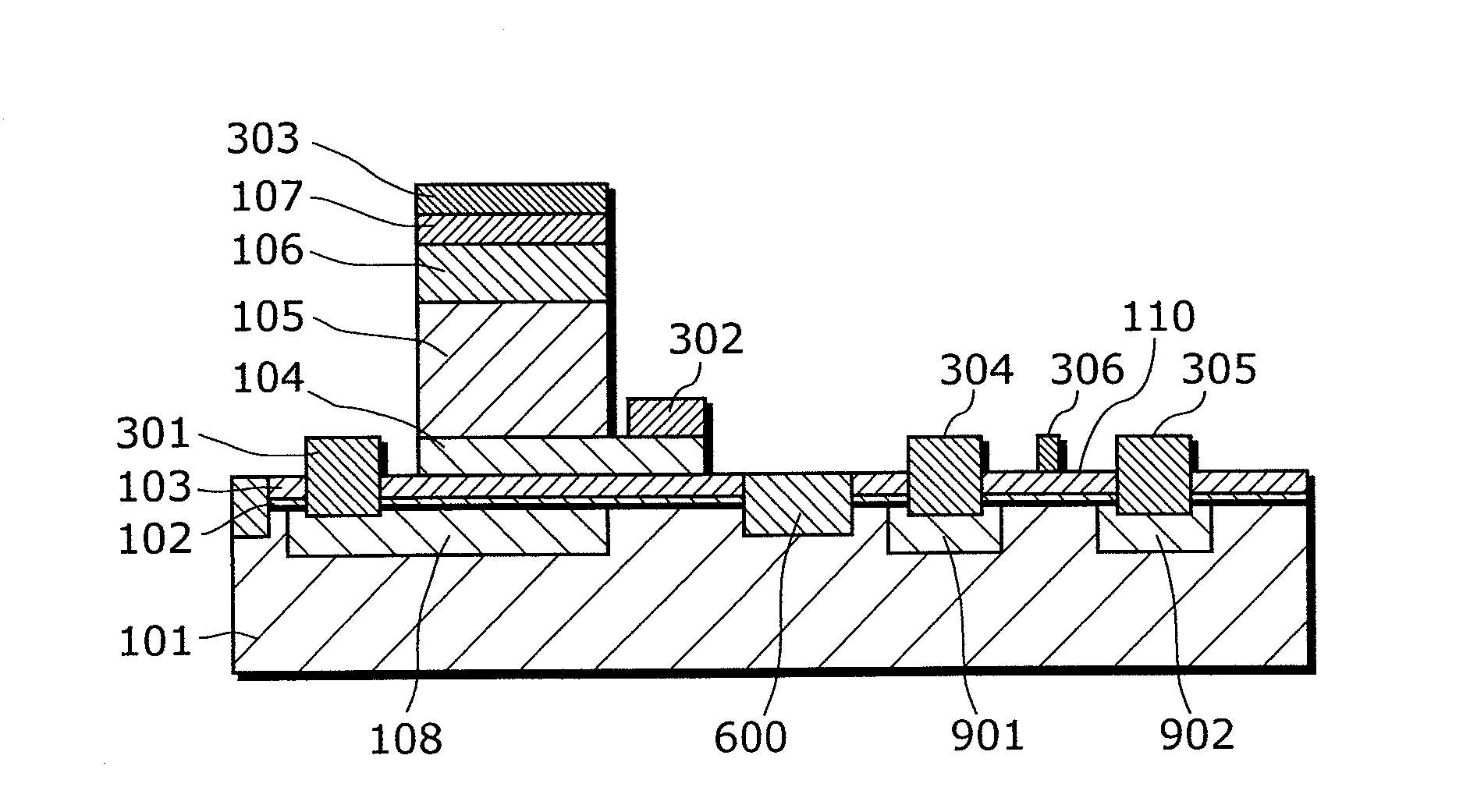
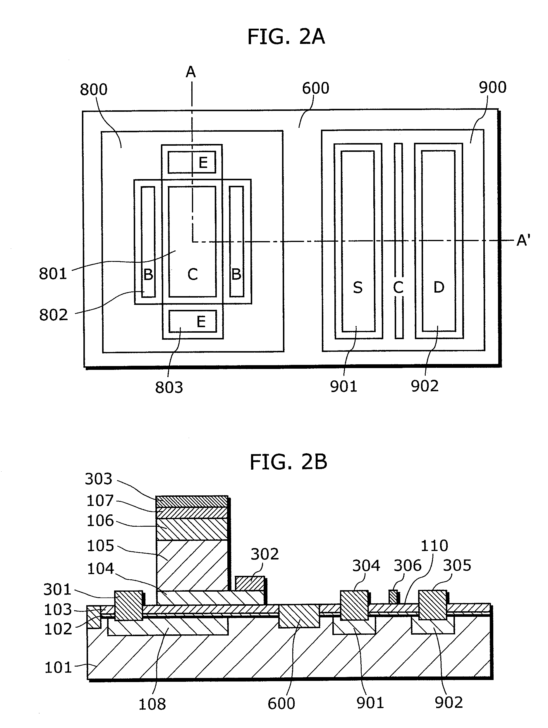
[0053]FIG. 2A is an overhead diagram which shows the structure of the HBT and HFET integrated circuit according to the first embodiment of the present invention. FIG. 2B is a cross section diagram which shows the structure of the same integrated circuit (the cross section diagram along the line A-A′ in FIG. 2A).

[0054]The integrated circuit includes a region (HBT region) 800 which functions as a collector-up type HBT, and a region (HFET region) 900 which functions as an HFET.

[0055]A channel layer 102 of a first conductivity, an emitter layer 103 of the first conductivity, a base layer 104 of a second conductivity with a band gap smaller than that of the emitter layer 103, a low impurity concentration collector layer 105 or a non-doped collector layer 105 which is of the first conductivity, a sub-collector layer 106 which is of the first conductivity and is doped with a impurity concentration higher than that of the collector layer 105, and a collector cap layer 107 on which a collect...

second embodiment

[0084]Next, a method for manufacturing the HBT and HFET integrated circuit according to the second embodiment of the present invention is described in detail using FIG. 4. FIG. 4 is a cross-section diagram for describing sequential steps of the method for manufacturing the integrated circuit.

[0085]First, the channel layer 102 made of InGaAs, in which an n-type uniformly doped layer or a δ doped layer is formed, is formed on the semi-insulating GaAs substrate 101 by epitaxial growth (FIGS. 4(a) and (b)).

[0086]Next, an ion species which functions as an n-type carrier such as an Se ion, is implanted in a predetermined region of the semi-insulating GaAs substrate 101 on which the emitter contact region 108, the source region 901, and the drain region 902 are to be formed on the semi-insulating GaAs substrate 101. For example, the ion species is implanted at an acceleration voltage of 30 keV and with a dose amount of 1×1014 cm−3.

[0087]Next, the region in which the ion species has been im...


PUM


Abstract

The object of the present invention is to provide a semiconductor device and the manufacturing method thereof which are capable of preventing decrease in the collector breakdown voltage and reducing the collector resistance. The semiconductor device according to the present invention includes: a HBT formed on a first region of a semiconductor substrate; and an HFET formed on a second region of the semiconductor substrate, wherein the HBT includes: an emitter layer of a first conductivity; a base layer of a second conductivity that has a band gap smaller than that of the emitter layer; a collector layer of the first conductivity or a non-doped collector layer; and a sub-collector layer of the first conductivity which are formed sequentially on the first region, and the HFET includes an electron donor layer including a part of the emitter layer, and a channel layer formed under the electron donor layer.

Description

BACKGROUND OF THE INVENTION[0001](1) Field of the Invention[0002]The present invention relates to an HBT and HFET integrated circuit (Bi-HFET) used as a high-frequency semiconductor device and to a manufacturing method thereof.[0003](2) Description of the Related Art[0004]Hetero-junction bi-polar transistors (HBT), which utilize semiconductors with large bandgaps in emitters, are high-frequency analogue devices used in cellular phones and the like. In particular, InGaP / GaAs HBTs that use InGaP in emitters have low temperature dependence, and methods of using InGaP / GaAs HBTs for highly reliable devices are expected to continually multiply.[0005]HBTs can be distinguished between an emitter-up type and a collector-up type. Generally, since the emitter-up type is superior to the collector-up type in processability, HBTs of the emitter-up type are presently mass produced. The HBTs of the collector-up type can decrease the base-collector capacity (Cbc) and is superior in this characterist...

Claims


Application Information

Patent Timeline
Patent Type & Authority Patents(United States)
IPC IPC(8): H01L31/0328
CPCH01L21/8252H01L27/0605H01L27/0623H01L21/8249
Inventor MURAYAMA, KEIICHITAMURA, AKIYOSHIMIYAMOTO, HIROTAKAMIYAJIMA, KENICHI
Owner COLLABO INNOVATIONS INC
Why Eureka
Try Eureka