Heat processing apparatus for semiconductor process
a technology of heat processing apparatus and semiconductor, which is applied in the direction of coating, chemical vapor deposition coating, metallic material coating process, etc., can solve the problems of particle contamination, difficult to form films with high uniformity among the target substrates, and increase the gap between the reaction tube and the target substrate, so as to achieve the effect of improving the planar uniformity of the film thickness
- Summary
- Abstract
- Description
- Claims
- Application Information
AI Technical Summary
Benefits of technology
Problems solved by technology
Method used
Image

Examples
first embodiment
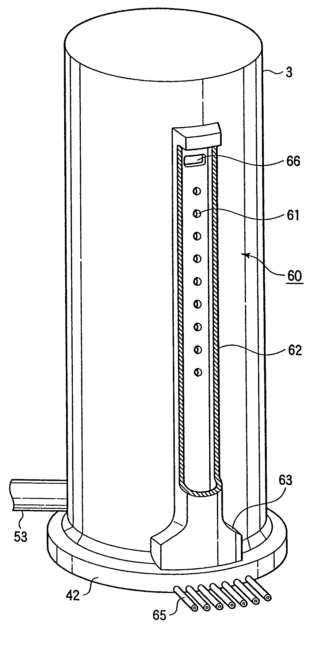
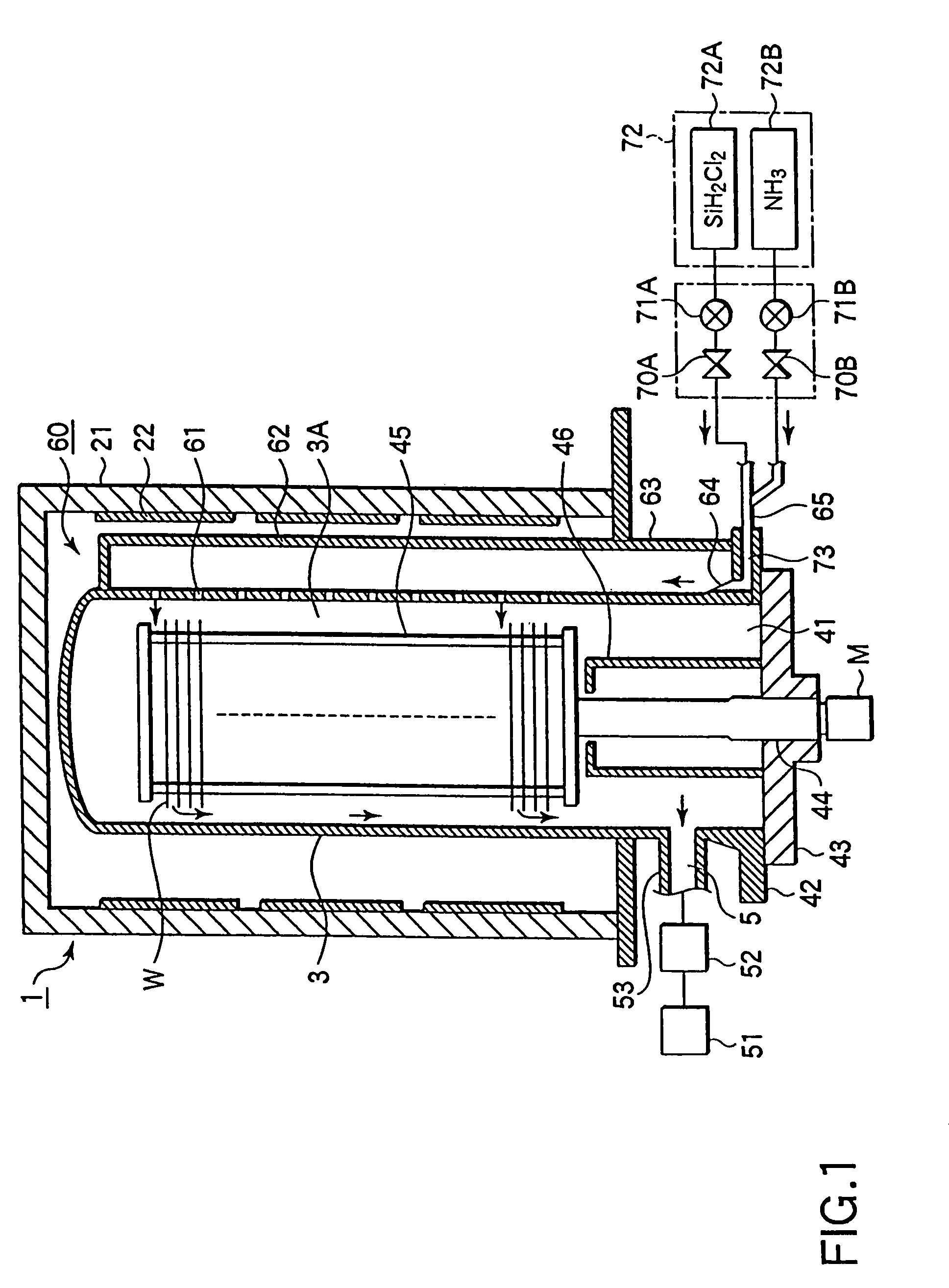
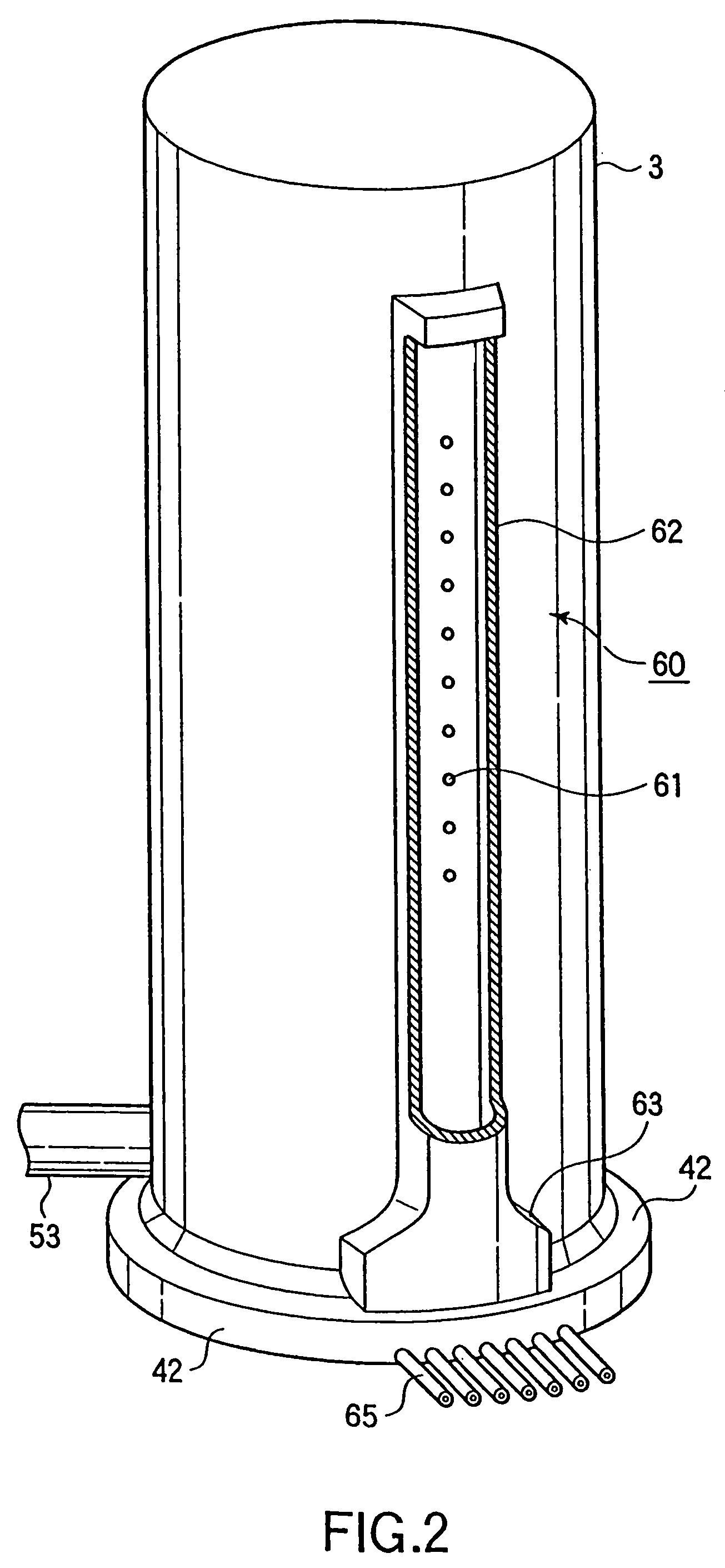
[0034]FIG. 1 is a sectional side view showing the overall arrangement of a heat processing apparatus for a semiconductor process according to the first embodiment of the present invention. This heat processing apparatus 1 has a cylindrical reaction tube 3 made of a heat-resistant insulating material, e.g., quartz, and having a circular section. The reaction tube 3 includes a process field 3A where semiconductor wafers W stacked at intervals are to be stored. The reaction tube 3 has an opening 41, serving as a transfer port, at its proximal end side (lower end side). A flange 42 integral with the reaction tube 3 is formed on the edge portion of the opening 41. The flange 42 engages with a lid 43 vertically moved by a boat elevator (not shown), so that the opening 41 can be hermetically closed.
[0035]A cylindrical cover 21 made of, e.g., a heat insulating material, surrounds the reaction tube 3. A plurality of heaters 22 are disposed along the inner wall surface of the cylindrical cove...
second embodiment
[0051]FIG. 6 is a sectional side view showing the overall arrangement of a heat processing apparatus for a semiconductor process according to the second embodiment of the present invention. FIG. 7 is a partially cutaway perspective view showing a reaction tube and a gas supply duct in the heat processing apparatus in FIG. 6. In this heat processing apparatus 1X, a gas supply duct 60 and gas delivery holes 61 are arranged in the same manner as in the heat processing apparatus 1 of the first embodiment. Above the uppermost gas delivery hole 61 in the gas supply duct 60 and above a process field 3A, a pressure equalization hole 66 communicating with the interior of a reaction tube 3 is formed. The pressure equalization hole 66 is formed so that process gases are supplied to a portion above a process field in the reaction tube 3 where wafers W are held. The pressure equalization hole 66 has an opening area larger than that of each gas delivery hole 61, and forms a substantially rectangu...
third embodiment
[0054]FIG. 8 is a sectional side view showing the overall arrangement of a heat processing apparatus for a semiconductor process according to the third embodiment of the present invention. FIG. 9 is a partially cutaway perspective view showing a reaction tube and a gas supply duct in the heat processing apparatus in FIG. 8. In this heat processing apparatus 1Y, a gas supply duct 60 extends from the bottom portion to the top portion of a reaction tube 3, as shown in FIG. 9 as well. In this case, the temperature of the lower portion of a process field 3A must be set higher than that of the upper portion by separately controlling, e.g., three heaters 22 that are divided in the vertical direction, so that a temperature gradient is formed in the process field 3A in the vertical direction. Therefore, this heat process is applied to a process in which temperature difference among wafers W does not influence the yield. An example of such a heat process includes a process of forming an SiO2 ...
PUM
| Property | Measurement | Unit |
|---|---|---|
| diameters | aaaaa | aaaaa |
| diameter | aaaaa | aaaaa |
| pressure | aaaaa | aaaaa |
Abstract
Description
Claims
Application Information
 - R&D
- Intellectual Property
- Life Sciences
- Materials
- Tech Scout
- Unparalleled Data Quality
- Higher Quality Content
- 60% Fewer Hallucinations
Browse by: Latest US Patents, China's latest patents, Technical Efficacy Thesaurus, Application Domain, Technology Topic, Popular Technical Reports.
© 2025 PatSnap. All rights reserved.Legal|Privacy policy|Modern Slavery Act Transparency Statement|Sitemap|About US| Contact US: help@patsnap.com