Holey electrode grids for photovoltaic cells with subwavelength and superwavelength feature sizes

a photovoltaic cell and feature size technology, applied in the field of solar or light energy, can solve the problems of limiting cell performance, limiting photovoltaic energy collection, and limiting the series resistance issu

Inactive Publication Date: 2011-10-18
GLOBALFOUNDRIES INC
View PDF37 Cites 7 Cited by
  • Summary
  • Abstract
  • Description
  • Claims
  • Application Information

AI Technical Summary

Benefits of technology

[0013]Embodiments of the invention use metal electrode to retain its very high conductivity (˜100× larger than best TCO), patterned into holey structures with subwavelength or superwavelength feature size while maintaining the same level of shadowing loss. Depending on the size of the holes and their periodicity, the invention can achieve significant benefits such as: reduced cell series resistance, as the metal grid has larger area coverage so the current transport are not limited by the (high) emitter sheet resistance anymore, and enhanced light transmission due to subwavelength electrode linewidth (that is invisible to light) or due to plasmonics effect.

Problems solved by technology

Despite good conversion efficiencies and long-term reliability, widespread energy collection using single-crystal silicon cells is thwarted by the exceptionally high cost of single crystal silicon material and interconnection processing.
Despite significant improvements in individual cell conversion efficiencies for both single crystal and thin film approaches, photovoltaic energy collection has been generally restricted to applications having low power requirements.
In all solar cells, especially the high performance ones, series resistance issue is a serious limiting factor for cell performance.
However such TCO film still has a limited conductivity and still contributes to considerable amount of series resistance.

Method used


Image

  • Holey electrode grids for photovoltaic cells with subwavelength and superwavelength feature sizes
  • Holey electrode grids for photovoltaic cells with subwavelength and superwavelength feature sizes
  • Holey electrode grids for photovoltaic cells with subwavelength and superwavelength feature sizes

Examples


Embodiment Construction

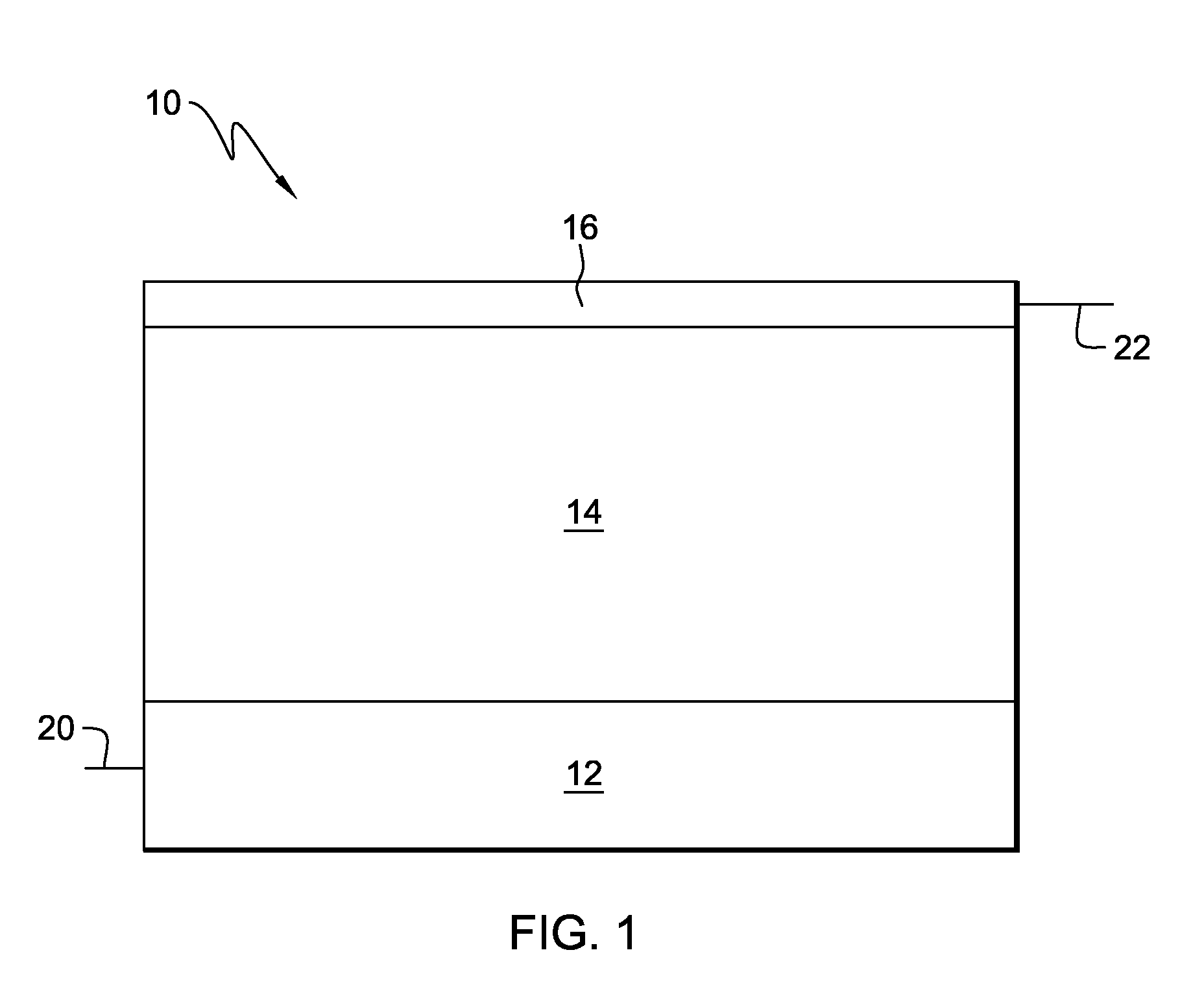
[0025]FIG. 1 is a diagram of a photovoltaic (PV) device, or solar cell, 10. The PV device 10 includes a back electrode layer 12, a PV material 14 and a front electrode 16. Light energy is transmitted to the PV layer 14, where it is absorbed and transformed into electric energy. The electricity generated within the PV device 10 migrates to either the front electrode 16 or the back electrode 12, from where it is directed out of the cell through an electrical contact 20 or 22. The PV layer 14 may be constructed of any among many different types of materials, including, but not limited to, semiconductor junctions, organic-dye based materials, photoelectrochemical cells, polymer solar cells, nanocrystal solar cells or dye sensitized solar cells, as well as other PV cell technologies.

[0026]More specifically, in the device of FIG. 1, the PV material 14 may be a semiconductor substrate comprised of a polycrystalline silicon but can also be a single-crystalline silicon, and it is of a p-type...


PUM


Abstract

A photovoltaic cell and a method of forming an electrode grid on a photovoltaic semiconductor substrate of a photovoltaic cell are disclosed. In one embodiment, the photovoltaic cell comprises a photovoltaic semiconductor substrate; a back electrode electrically connected to a back surface of the substrate; and a front electrode electrically connected to a front surface of the substrate. The substrate, back electrode, and front electrode form an electric circuit for generating an electric current when said substrate absorbs light. The front electrode is comprised of a metal grid defining a multitude of holes. These holes may be periodic, aperiodic, or partially periodic. The front electrode may be formed by depositing nanospheres on the substrate; forming a metallic layer on the substrate, around the nanospheres; and removing the nanospheres, leaving an electrode grid defining a multitude of holes on the substrate.

Description

BACKGROUND OF THE INVENTION[0001]1. Field of the Invention[0002]This invention generally relates to solar or light energy, and more specifically, the invention relates to photovoltaic cells.[0003]2. Background Art[0004]Solar energy has long been looked to as a significant part of a solution to the ever increasing energy needs of the planet's population. Increasing costs of mining fossil fuels and increased concerns over “greenhouse” emissions have furthered interest in exploiting alternative energy strategies, including solar energy sources. To date, solar energy conversion has generally relied upon either the direct harvesting of solar thermal energy, e.g., in heating applications, or in thermoelectric conversion, or through the direct conversion of photonic energy to electrical energy through the use of photovoltaic cells.[0005]Photovoltaic cells have developed according to two distinct methods. The initial operational cells employed a matrix of single crystal silicon appropriatel...

Claims


Application Information

Patent Timeline
Patent Type & Authority Patents(United States)
IPC IPC(8): H01L21/44
CPCH01L31/022433Y02E10/50
Inventor GUHA, SUPRATIKGUNAWAN, OKI
Owner GLOBALFOUNDRIES INC
Why Eureka
Try Eureka