Solid-state image sensing device

a sensing device and solid-state technology, applied in the direction of radio frequency controlled devices, instruments, television systems, etc., to achieve the effect of high sn ratio, no deterioration of resolution, and good color reproducibility

Inactive Publication Date: 2011-10-25
KK TOSHIBA
View PDF12 Cites 11 Cited by
  • Summary
  • Abstract
  • Description
  • Claims
  • Application Information

AI Technical Summary

Benefits of technology

[0010]The present invention has been made in view of the foregoing problem, and is directed to provide a solid-state image sensing device which has a high SN ratio with respect to a low-illumination subject and which has good color reproducibility and which causes no deterioration of resolution and no generation of aliasing even in the case of a subject having an edge.

Problems solved by technology

However, JP-A 2004-304706 (kokai) does not disclose any procedure for processing white pixel data, and gives no consideration to the processing of a pixel signal corresponding to an edge having rapidly changing luminance such as a subject at a high spatial frequency.

Method used


Image

  • Solid-state image sensing device
  • Solid-state image sensing device
  • Solid-state image sensing device

Examples


first embodiment

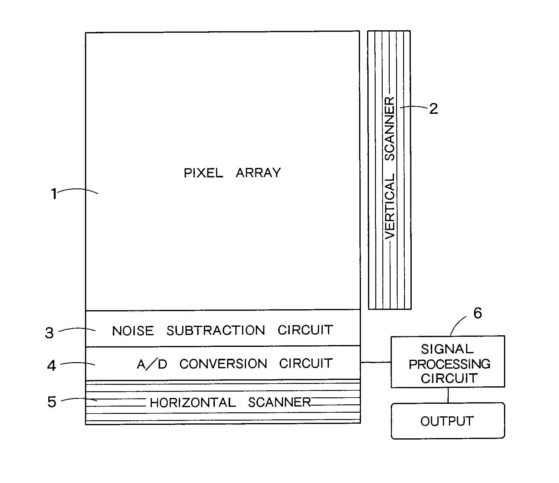
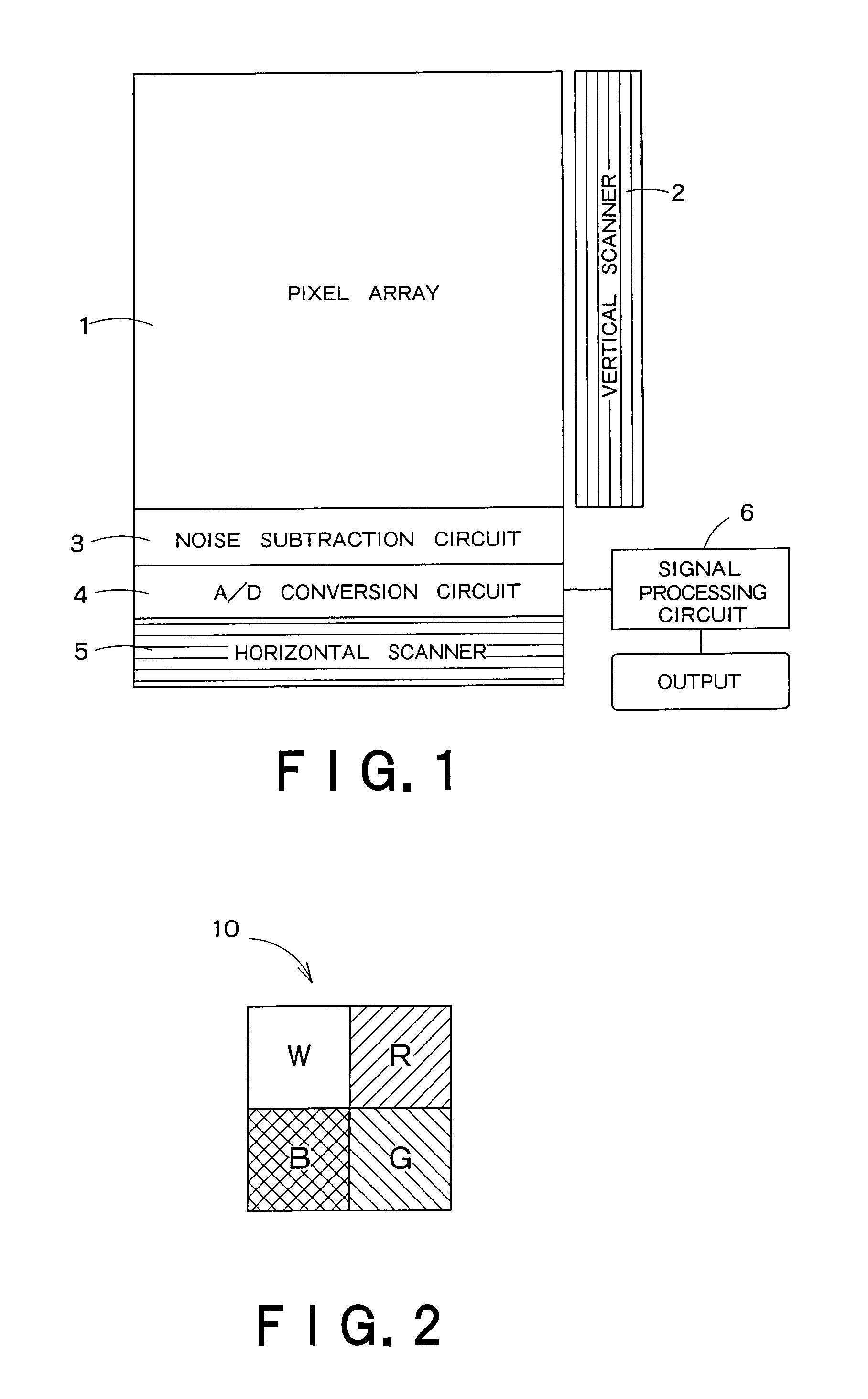
[0063]FIG. 1 is a block diagram showing a schematic configuration of a solid-state image sensing device according to one embodiment of the present invention. The solid-state image sensing device in FIG. 1 has a pixel array 1 in which a plurality of pixels having photoelectric conversion elements are arranged in matrix form, a vertical scanner 2 for sequentially supplying drive voltages to the respective rows in the pixel array 1, a noise subtraction circuit 3 for removing noise contained in an imaging signal photoelectrically converted in the individual pixel, an A / D conversion circuit 4 for the A / D conversion of the imaging signal output from the noise subtraction circuit 3, a horizontal scanner 5 for sequentially selecting imaging data after the A / D conversion row by row and reading the imaging data, and a signal processing unit 6 for performing signal processing described later with respect to the imaging data.

[0064]The imaging data is serially input to the signal processing unit...

second embodiment

[0118]A second embodiment is different from the first embodiment in the kind of pixel line used for an edge judgment.

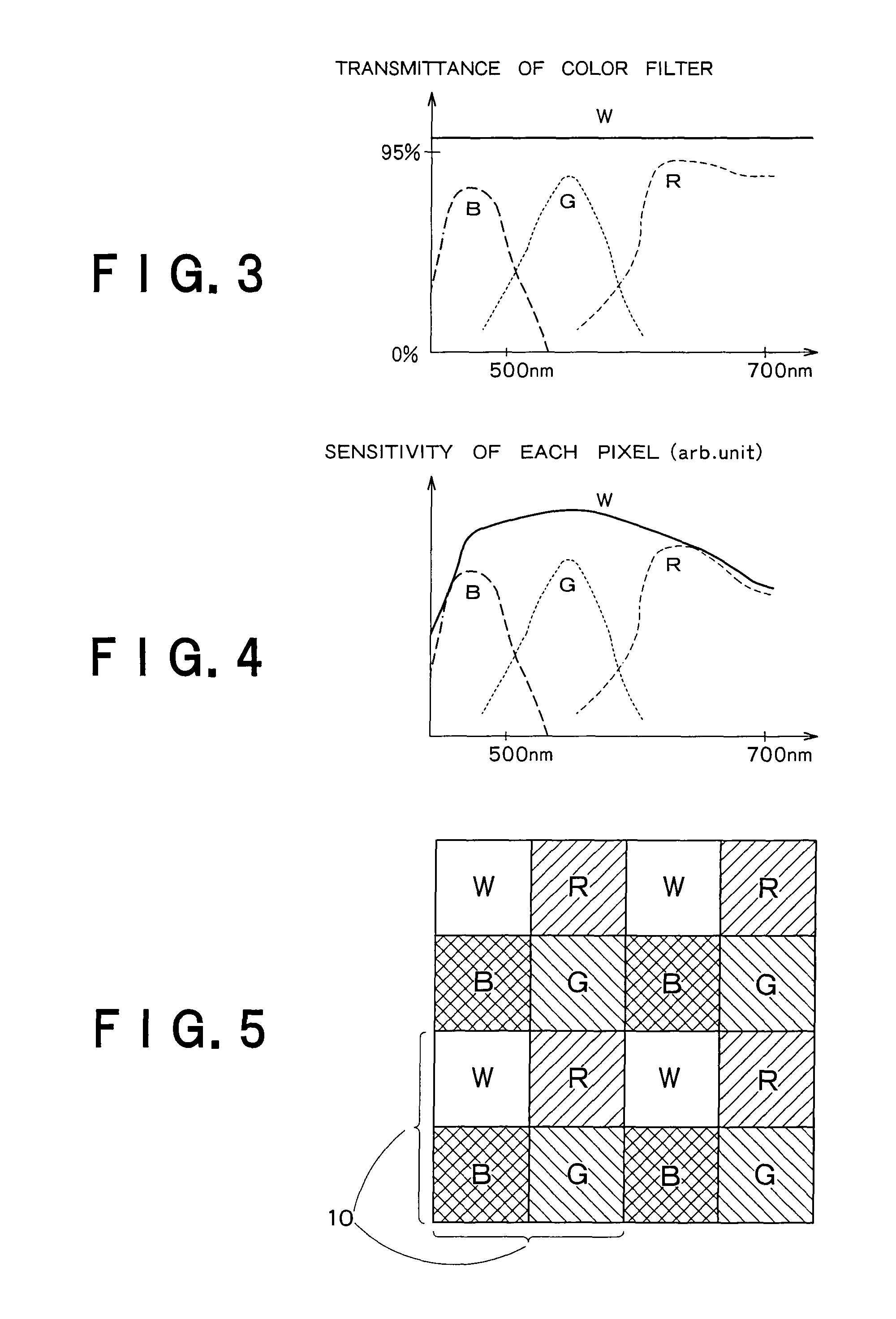
[0119]In the example described in the first embodiment, as shown in FIG. 14(a) to FIG. 14(d) or FIG. 15(a) to FIG. 15(d), three lines are set as comparison targets for edge detection in a pixel block, and the central line among these lines includes a W pixel targeted for signal processing located in the center of the pixel block.

[0120]The pixel line targeted for comparison does not necessarily have to include the W pixel targeted for signal processing located in the center of the pixel block. Thus, in the second embodiment described below, the edge judgment is carried out using two lines adjacent to the central W pixel. Moreover, the second embodiment is characterized in that the kind of two pixel lines targeted for comparison is the same.

[0121]FIG. 16 is a flowchart showing a processing operation of a signal processing unit 6 configured as in FIG. 12 in the second em...

third embodiment

[0127]In a third embodiment, a region having no edge is detected around a target W pixel, and color separation processing is performed in this region.

[0128]FIG. 18 is a flowchart showing the processing operation of a signal processing unit 6 according to the third embodiment, and FIG. 19(a) to FIG. 19(c) are diagrams explaining pixel lines used in an edge judgment.

[0129]First, a color pixel value in a pixel block including a W pixel in the center is acquired (step S21). Then, the central W pixel is used as a pixel targeted for signal processing to calculate the total of the color pixel values of a vertical line LineV0 including the W pixel, the total of the color pixel values of each of two vertical lines LineV1, LineV2 located on both sides of the vertical line LineV0 across one pixel, the total of the color pixel values of a horizontal line LineH0 including the W pixel, the total of the color pixel values of each of two horizontal lines LineH1, LineH2 located on both sides of the ...


PUM


Abstract

A solid-state image sensing device has a plurality of pixels, a read-out circuit for reading out electric signals obtained by the photoelectric conversion element, and a signal processing unit for performing signal processing for the electric signal read out from the read-out circuit. The plurality of pixels include a first pixel having a transparent film, a plurality of second pixels each having a first color filter, a plurality of third pixels each having a second color filter, and a plurality of fourth pixels each having a third color filter. The signal processing unit has a color acquisition unit for acquiring a white pixel value and first to third color pixel values, an edge judgment unit, a color separation unit and a single color pixel calculation unit.

Description

CROSS REFERENCE TO RELATED APPLICATIONS[0001]This application is based upon claims the benefit of priority from the prior Japanese Patent Application No. 2007-150608, filed on Jun. 6, 2006, the entire contents of which are incorporated herein by reference.BACKGROUND OF THE INVENTION[0002]1. Field of the Invention[0003]The present invention relates to a solid-state image sensing device in which a plurality of pixels having photoelectric conversion elements are arranged in matrix form.[0004]2. Related Art[0005]Recently, CMOS image sensors have been actively developed. In particular, along with the miniaturization in a semiconductor process (reduction in design rules), a single-chip color image sensor has been commercialized in which the number of pixels exceeds five millions at a pixel pitch of, for example, 2.0 μm.[0006]However, the trend of the pixel miniaturization is shifting toward a level with a pixel pitch of 1.7 μm and an aperture area or 1 μm or less. In such a pixel size, th...

Claims


Application Information

Patent Timeline
Patent Type & Authority Patents(United States)
IPC IPC(8): H04N3/14H04N5/335H04N9/083H04N9/04H01L27/146H04N9/07
CPCG06T3/4015H04N9/045H04N25/133H04N25/135H04N23/843
Inventor HONDA, HIROTOILDA, YOSHINORIEGAWA, YOSHITAKA
Owner KK TOSHIBA
Why Eureka
Try Eureka