Method and system for screening nets in a post-layout environment

Inactive Publication Date: 2011-11-15
CADENCE DESIGN SYST INC
View PDF4 Cites 13 Cited by
  • Summary
  • Abstract
  • Description
  • Claims
  • Application Information

AI Technical Summary

Benefits of technology

[0011]An object of the present invention is to provide a method for screening routed nets in a post-layout circuit environment, wherein signal channels corre

Problems solved by technology

A typical circuit layout will easily include thousands of such nets, even hundreds of thousands; yet, adequate verification cannot be had without the reliable identification and remedy of individual nets having faults.
Pervasive timing problems are generated if they are out of phase.
This presents a formidable challenge in applications where thousands of nets are presented for verificat

Method used


Image

  • Method and system for screening nets in a post-layout environment
  • Method and system for screening nets in a post-layout environment
  • Method and system for screening nets in a post-layout environment

Examples


Embodiment Construction

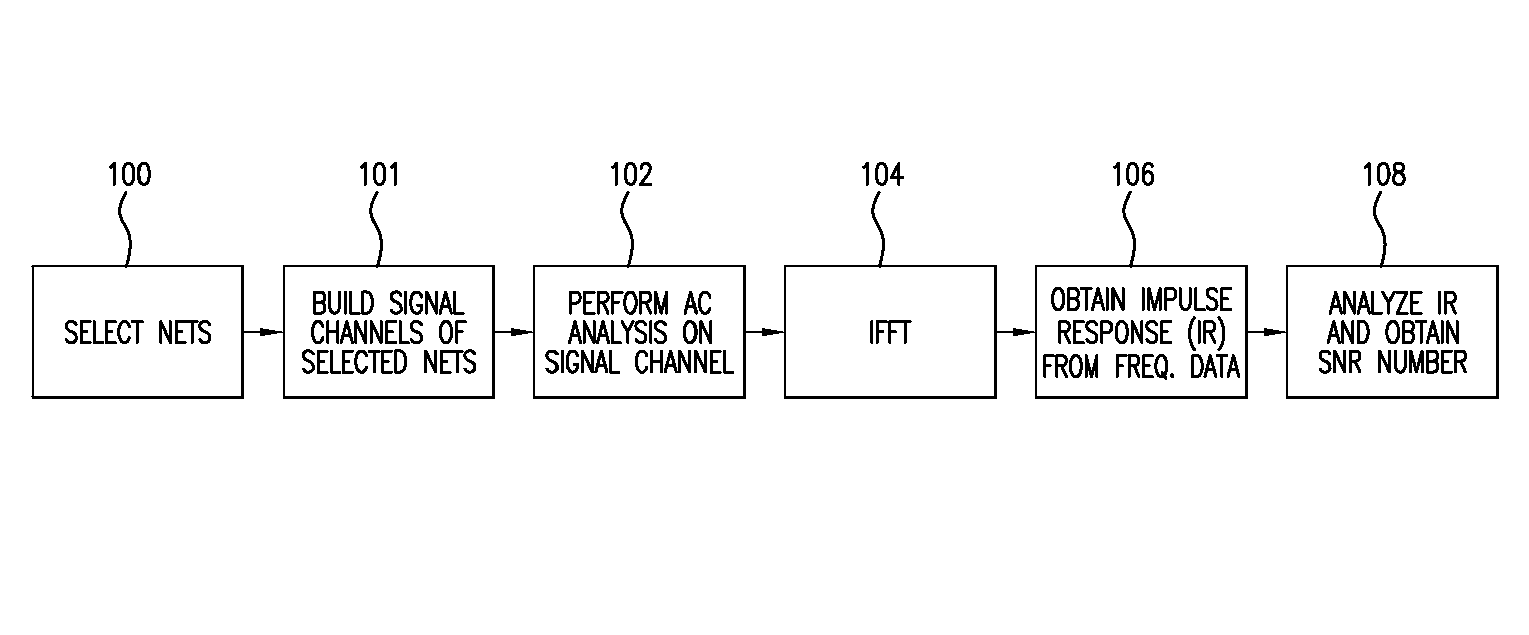
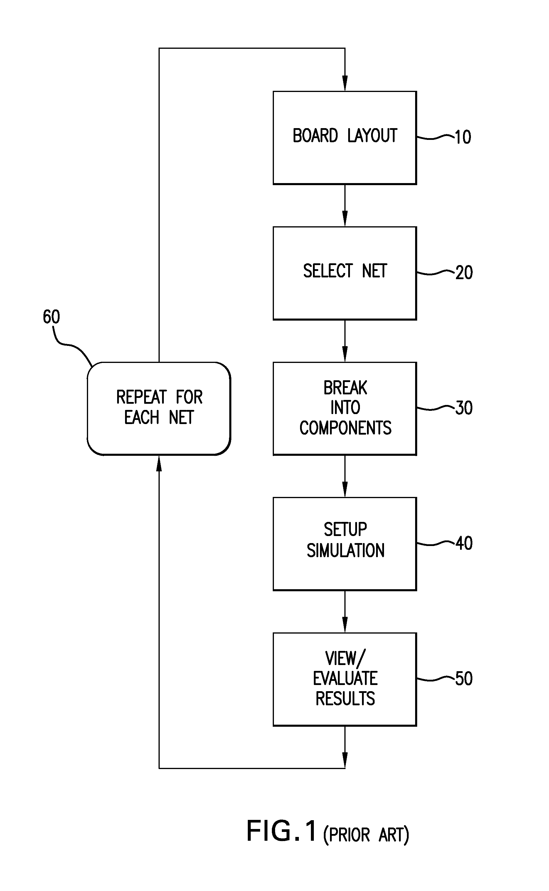
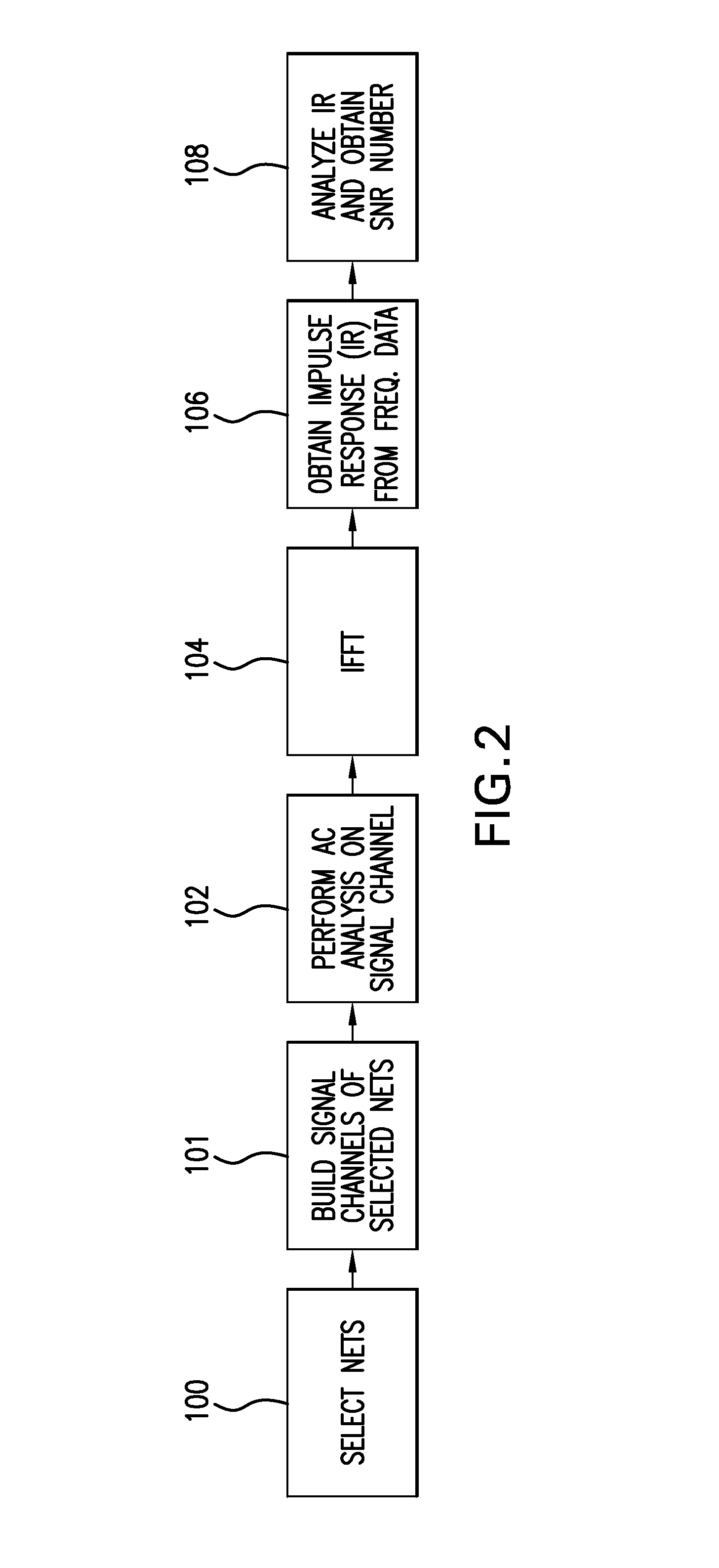
[0026]Conventional methods of determining signal channel quality in high speed circuit applications include application of Time Domain Reflectometry (TDR). In TDR, signal energy is input to a system and propagated through a channel. For instance, the input may be a signal source originating from a driver component, such as an active electrical element like a transistor. The signal energy will encounter various physical discontinuities along the channel. These discontinuities may take the form of both active and passive circuit elements, physical portions of a circuit board such as vias, conductors, etc. For example, a signal may begin at a driver which may be in the form of an I / O buffer integrated within an IC, traverse its package parasitics, continue through its pin parasitics to the circuit board, then through routed net material such as a printed conductor. The signal may also pass through vias in the board between levels, then through a connector, another net, possibly another...


PUM


Abstract

A method and systems are provided for screening and rapid evaluation of routed nets in a post-layout circuit environment, such as in the design of printed circuit boards. A portion of nets are selected for determination of associated signal quality factors. Signal channels containing one or more selected nets are then built. A reference input stimulus is propagated along each of the signal channels in a frequency based simulation for generating characteristic responses of the selected nets' signal channels. A signal channel quality factor is obtained for each signal channel based upon its characteristic response. The signal channels and their nets are then comparatively analyzed according to corresponding signal channel quality factors to selectively identify any aberrant nets warranting supplemental evaluation for faults.

Description

BACKGROUND OF THE INVENTION[0001]1. Field of the Invention[0002]The present invention is generally directed to a method and system for screening nets of circuit design in a post-layout environment. More specifically, the present invention is directed to a method and system operable during design verification for quickly and conveniently screening routed nets of a circuit layout, such as in a printed circuit board design, for potentially faulty nets warranting further evaluation.[0003]2. Description of the Related Art[0004]Typically, when a board level circuit layout has been designed (all circuit elements, including devices, discrete components, conductive traces, and the like have been placed and routed), it undergoes post-layout test / verification using a simulation tool.[0005]The circuit layout at this stage defines a collection of nets, each forming a connection directly between circuit component pins. One or more nets are encompassed by a signal transmitting channel extending to...

Claims


Application Information

Patent Timeline
IPC IPC(8): G06F17/50
CPCG06F17/5036G06F2217/82G06F30/367G06F2119/10
Inventor VARMA, AMBRISHAL-HAWARI, FERASKESHAVAN, KUMAR
Owner CADENCE DESIGN SYST INC
Why Eureka
Try Eureka