Pulse width modulation circuit and class-D amplifier comprising the PWM circuit

a technology of pulse width and modulation circuit, which is applied in the direction of pulse technique, amplifier with semiconductor devices/discharge tubes, low frequency amplifiers, etc., can solve the problems of gate-oxide capacitors on the other hand having high capacitance per area but suffering from non-linearity

Active Publication Date: 2011-11-29
NXP BV
View PDF13 Cites 4 Cited by
  • Summary
  • Abstract
  • Description
  • Claims
  • Application Information

AI Technical Summary

Benefits of technology

[0010]It is an object of the invention to provide a PWM circuit of the type defined in the opening paragraph and a Class-D amplifier of the type defined in the second paragraph, in which the disadvantages defined above are avoided.
[0014]The characteristic features according to the invention provide the advantage that the use of non-linear gate-oxide capacitors in the integrators is allowed without degrading performance. Since non-linear gate-oxide capacitors require less area in integrated circuits than linear capacitors smaller and cheaper integrated circuits can be designed.
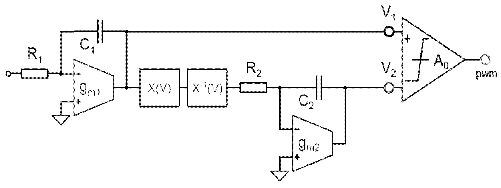
[0017]A second essential feature of the invention is that this potential instability is avoided by making the value of the resistor connecting the two integrators to be non-linear in a way related to the capacitor non-linearity.
[0019]Implementing the feedback capacitors of the integrators as non-linear gate-oxide capacitors results in small and reliable integrated circuits. Connecting PMOS and NMOS gate-oxide capacitors in parallel results in a smoother overall capacitance.
[0021]In a simple and easy to implement embodiment the circuit with an inversely non-linear factor X−1(V) comprises two anti-parallel connected diodes being serially connected to a first resistor, a second resistor bypassing the anti-parallel diodes and the first resistor.

Problems solved by technology

Unfortunately linear capacitors in IC processes tend to be large.
Gate-oxide capacitors on the other hand have high capacitance per area but suffer from non-linearity.

Method used


Image

  • Pulse width modulation circuit and class-D amplifier comprising the PWM circuit
  • Pulse width modulation circuit and class-D amplifier comprising the PWM circuit
  • Pulse width modulation circuit and class-D amplifier comprising the PWM circuit

Examples


Embodiment Construction

[0041]It will now be explained in detail how to build and use the present invention. First, reference is made to FIG. 5 showing the capacitance C of a gate capacitor of a PMOS transistor as a function of gate voltage VG with drain and source short-circuited. As can be seen from FIG. 5 the capacitance value C drops significantly near zero gate voltage. In this region the silicon underneath the gate-oxide is in depletion. For positive gate voltages VG the gate starts attracting electrons that form a so-called accumulation layer near the oxide interface. For negative voltages lower than the PMOS threshold voltage VTp an inversion layer consisting of holes is formed near the oxide interface. In both accumulation and inversion the capacitance C converges to:

[0042]Cox=W·L·ɛt-❘

[0043]where W and L are the width and length of the PMOS gate, tox is the thickness of the gate-oxide and εox is the permittivity of silicon-dioxide.

[0044]For NMOS transistors the gate capacitance looks similar but i...


PUM


Abstract

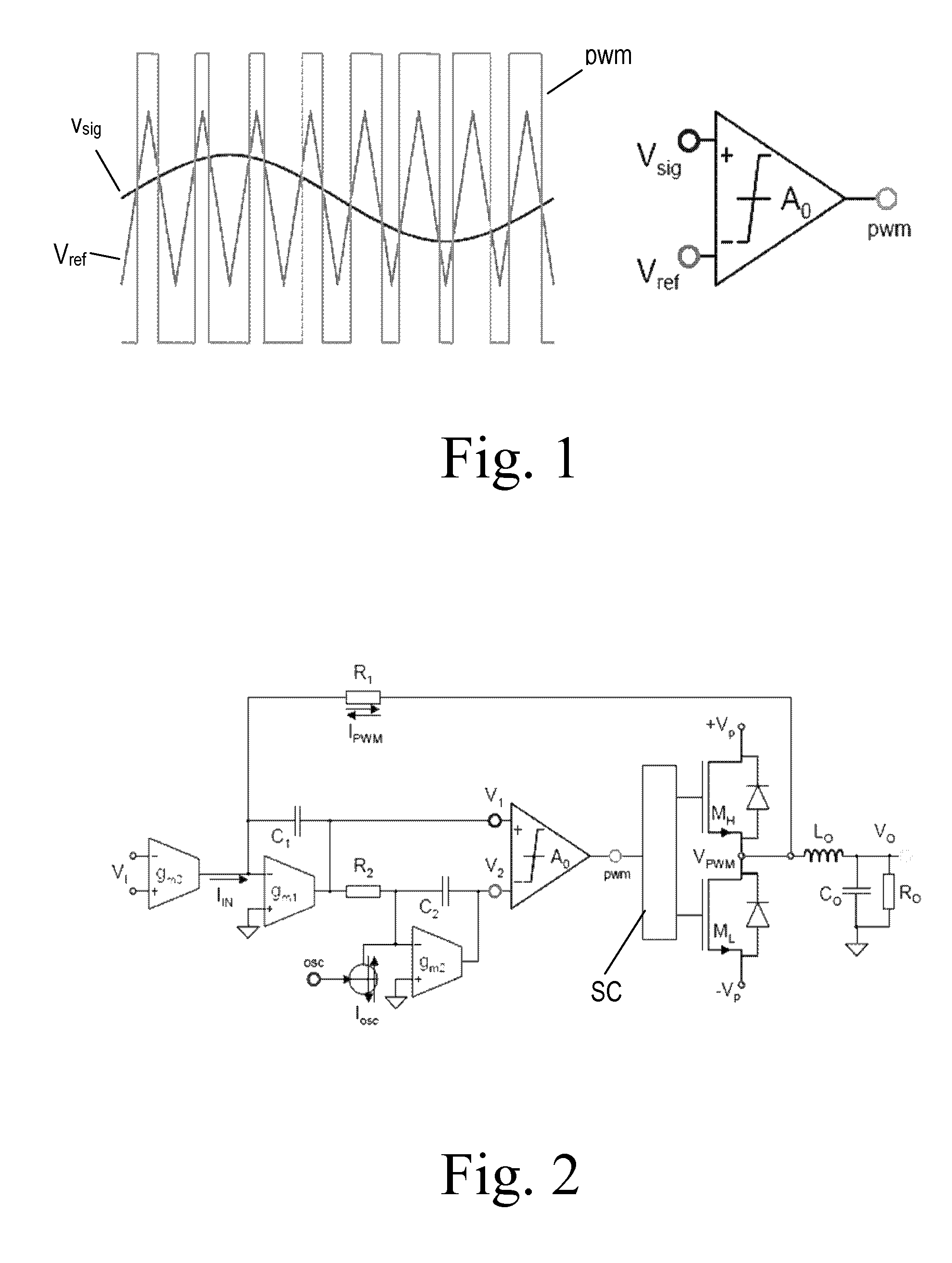
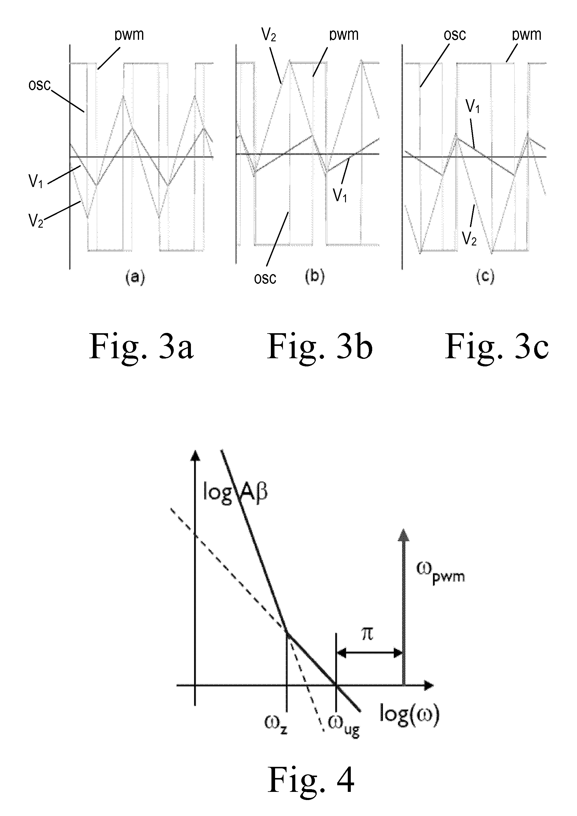
A pulse width modulation (PWM) circuit comprises a first integrator (g m1) with a first feedback capacitor (C1), a second integrator (gm1) with a second feedback capacitor (C2) and a comparator (A0) having a first input (V1) connected to the output of the first integrator (gm1) and a second input (V2) connected to the output of the second integrator (gm2). A connection path comprising a resistor (R2) is established from the output of the first integrator (gm1) to an input of the second integrator (gm2). The first and second feedback capacitors (C1, C2) have capacities with a non-linear factor X(V) and a circuit with an inversely non-linear factor X−1(V) is arranged in the connection path between the output of the first integrator (gm1) and said input of the second integrator (gm2). The PWM circuit may form path of a Class-D amplifier.

Description

FIELD OF THE INVENTION[0001]The invention relates to a pulse width modulation (PWM) circuit comprising a first integrator with a first feedback capacitor, a second integrator with a second feedback capacitor and a comparator having a first input connected to the output of the first integrator and a second input connected to the output of the second integrator, wherein a connection path comprising a resistor is established from the output of the first integrator to an input of the second integrator.[0002]The invention further relates to a Class-D amplifier.BACKGROUND OF THE INVENTION[0003]In most Class-D amplifiers some form of pulse-width modulation (PWM) is applied. A PWM signal can be constructed feed-forward by simply comparing the input signal Vsig with a triangular reference wave Vref as shown in FIG. 1. Usually the frequency of the reference wave Vref is much higher than that of the input signal Vsig.[0004]Ideally, the spectrum of the PWM signal does not contain harmonics of t...

Claims


Application Information

Patent Timeline
Patent Type & Authority Patents(United States)
IPC IPC(8): H03F3/38
CPCH03F1/3205H03F3/187H03F3/2171H03K7/08H03F2200/264H03F2200/351H03F2200/03
Inventor BERKHOUT, MARCOKRABBENBORG, BENNO
Owner NXP BV
Why Eureka
Try Eureka