

Phase shift keyed modulation of optical signal using chirp managed laser
a technology of managed laser and optical signal, applied in electromagnetic transmission, electrical apparatus, electromagnetic transceivers, etc., to achieve the effect of reducing the complexity of implementation, reducing the sampling rate, and increasing the precision of analog-to-digital converters
- Summary
- Abstract
- Description
- Claims
- Application Information
AI Technical Summary
Benefits of technology
Problems solved by technology
Method used
Image

Examples
Embodiment Construction
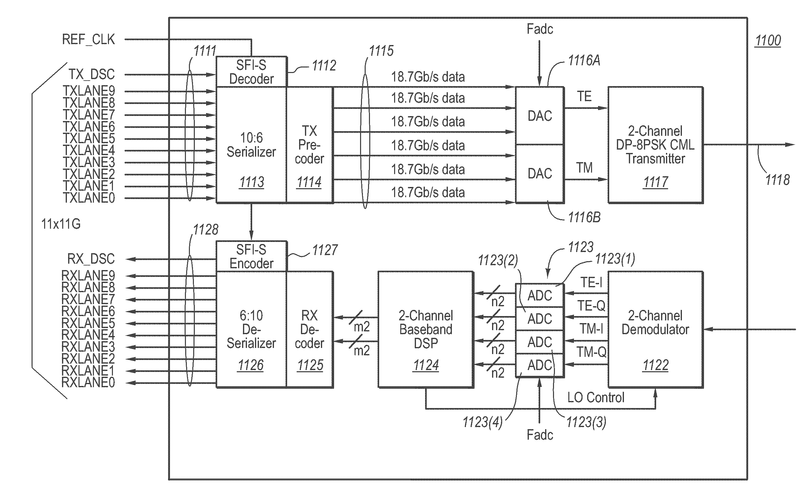
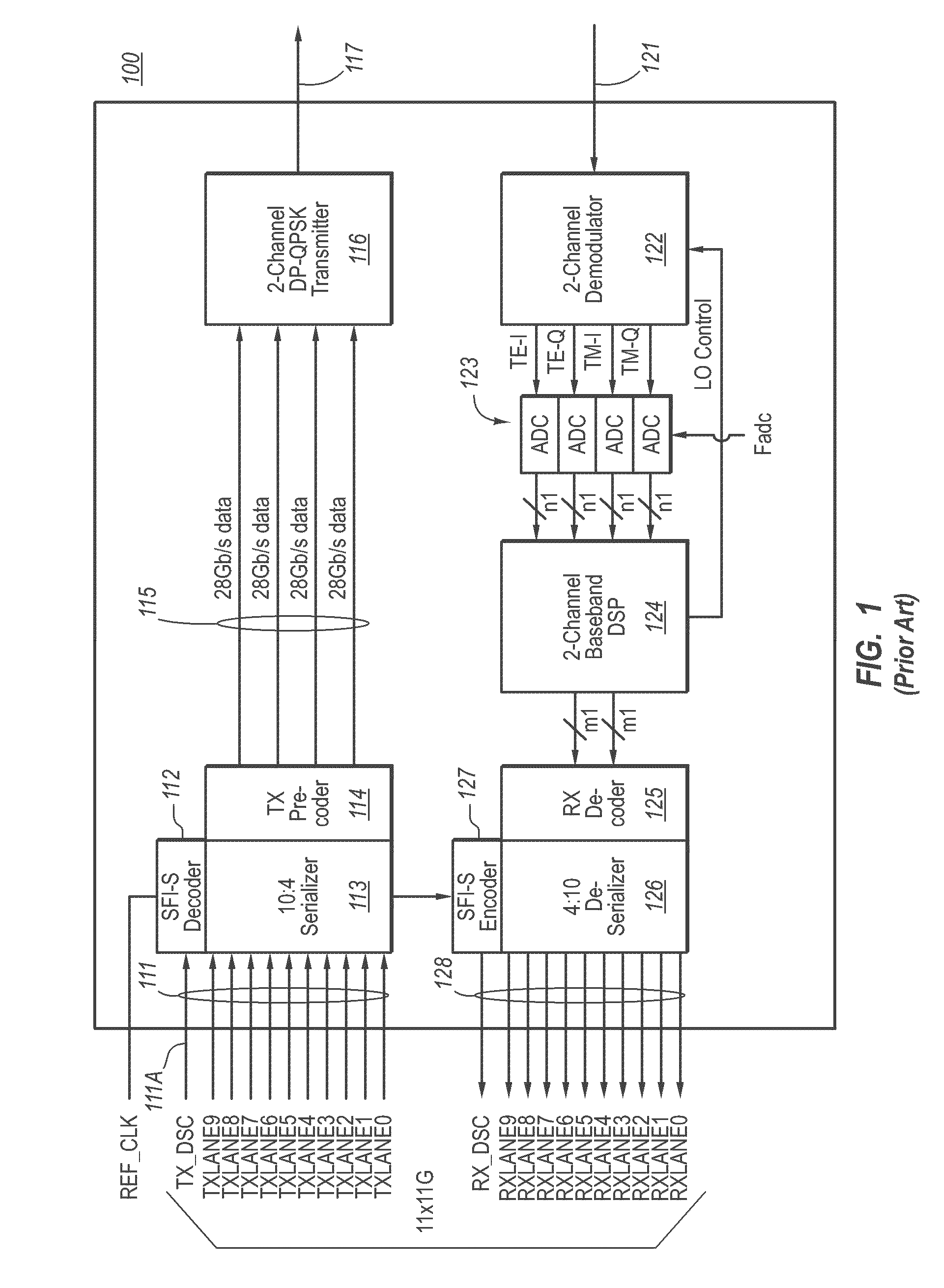
[0052]A high-speed optical transmitter and receiver structure are described herein. The high-speed optical transmitter comprises multiple digital lanes that are provided to a bank of digital-to-analog converters. The analog signals are then used to perform complex Phase Shift Keyed (PSK) modulation using both the in-phase and quadrature phase modulations, using a Chirp Managed Laser (CML)-based transmitter, and potentially using dual polarization (e.g., using the TE polarization and the TM polarization). A corresponding optical receiver receives the sequence of optical signals at a demodulator. For each polarization, the demodulator includes a corresponding demodulation channel that is configured to demodulate that polarization component of the optical signal into one or more analog signal components. Each of these analog signal components is converted into a corresponding digital signal using a corresponding analog-to-digital converter. The use of a CML transmitter may significantl...
PUM
 Abstract
Description
Claims
Application Information