Nanometer-scale transistor architecture providing enhanced carrier mobility

a transistor and nanometer-scale technology, applied in transistors, solid-state devices, thermoelectric devices, etc., can solve the problems of significant process complexity, reliability, cost, and complexity, and achieve enhanced carrier mobility, reduced scattering of electrons or holes traveling through the channel, and reduced the effect of the exten

a transistor and nanometer-scale technology, applied in transistors, solid-state devices, thermoelectric devices, etc., can solve the problems of significant process complexity, reliability, cost, and complexity, and achieve enhanced carrier mobility, reduced scattering of electrons or holes traveling through the channel, and reduced the effect of the exten

US8097922B1Active Publication Date: 2012-01-17RGT UNIV OF CALIFORNIA

Image

  • Nanometer-scale transistor architecture providing enhanced carrier mobility
  • Nanometer-scale transistor architecture providing enhanced carrier mobility
  • Nanometer-scale transistor architecture providing enhanced carrier mobility

Examples


Embodiment Construction

[0016]The embodiments set forth below represent the necessary information to enable those skilled in the art to practice the invention and illustrate the best mode of practicing the invention. Upon reading the following description in light of the accompanying drawing figures, those skilled in the art will understand the concepts of the invention and will recognize applications of these concepts not particularly addressed herein. It should be understood that these concepts and applications fall within the scope of the disclosure and the accompanying claims.

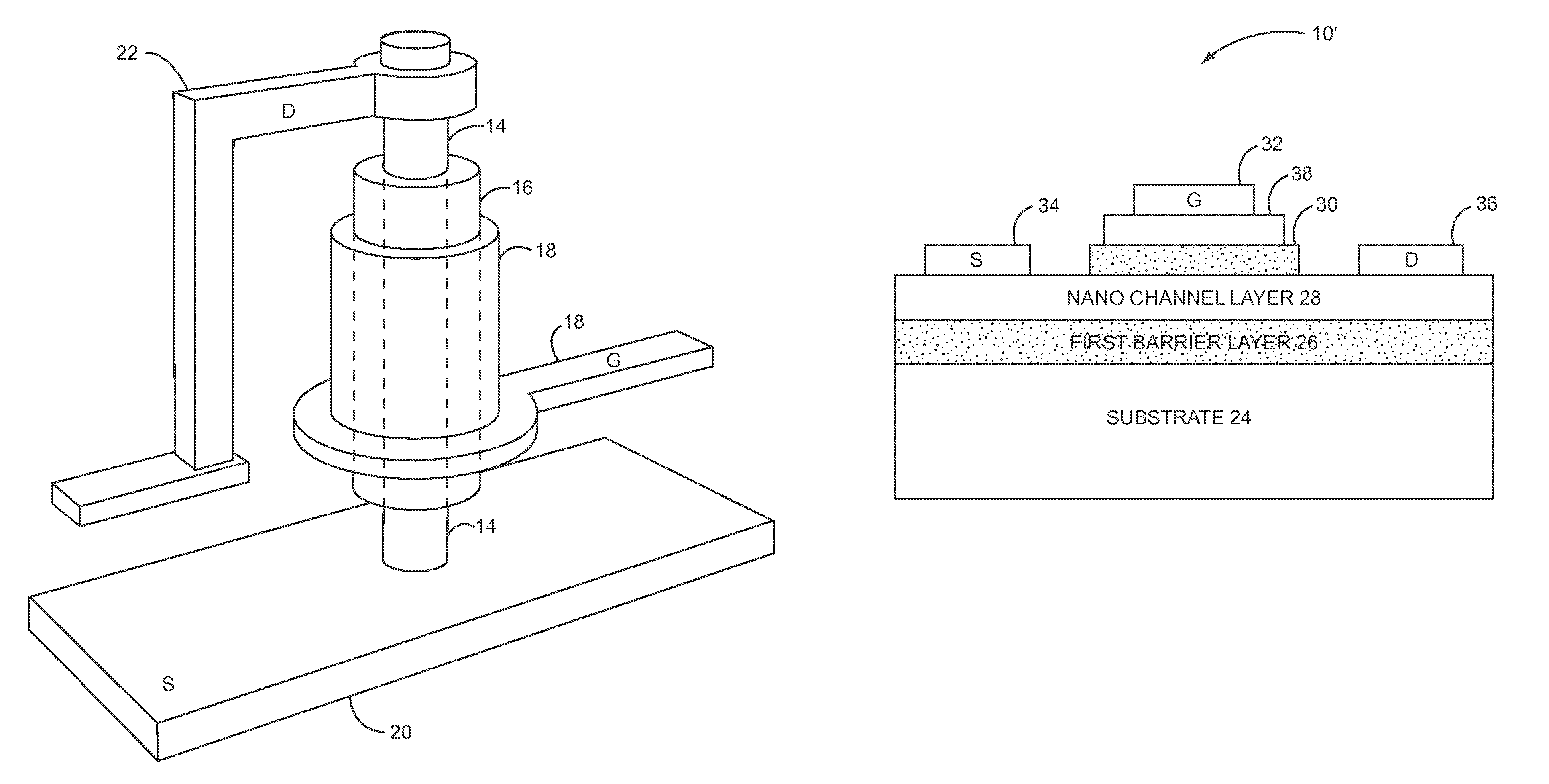
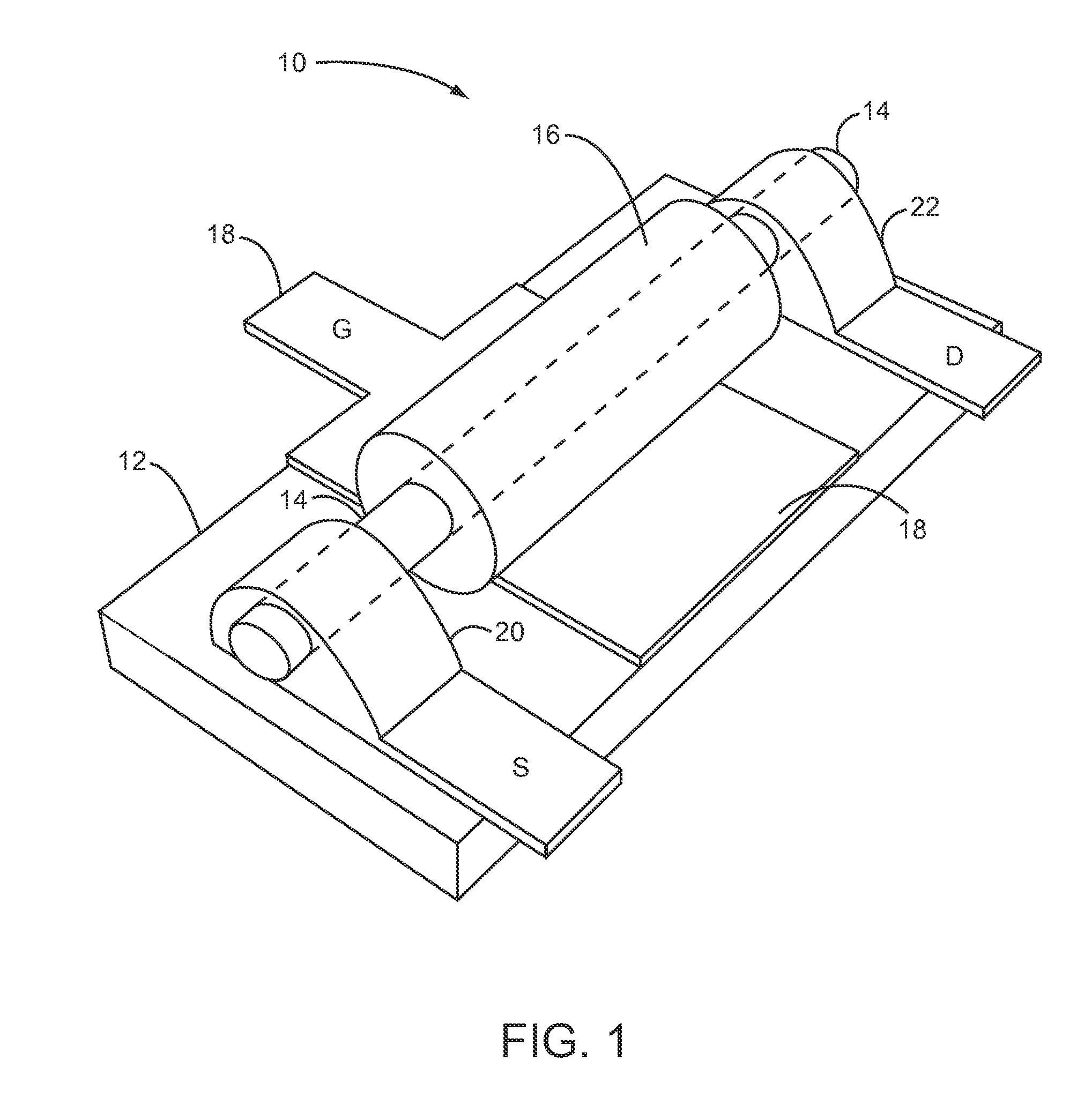
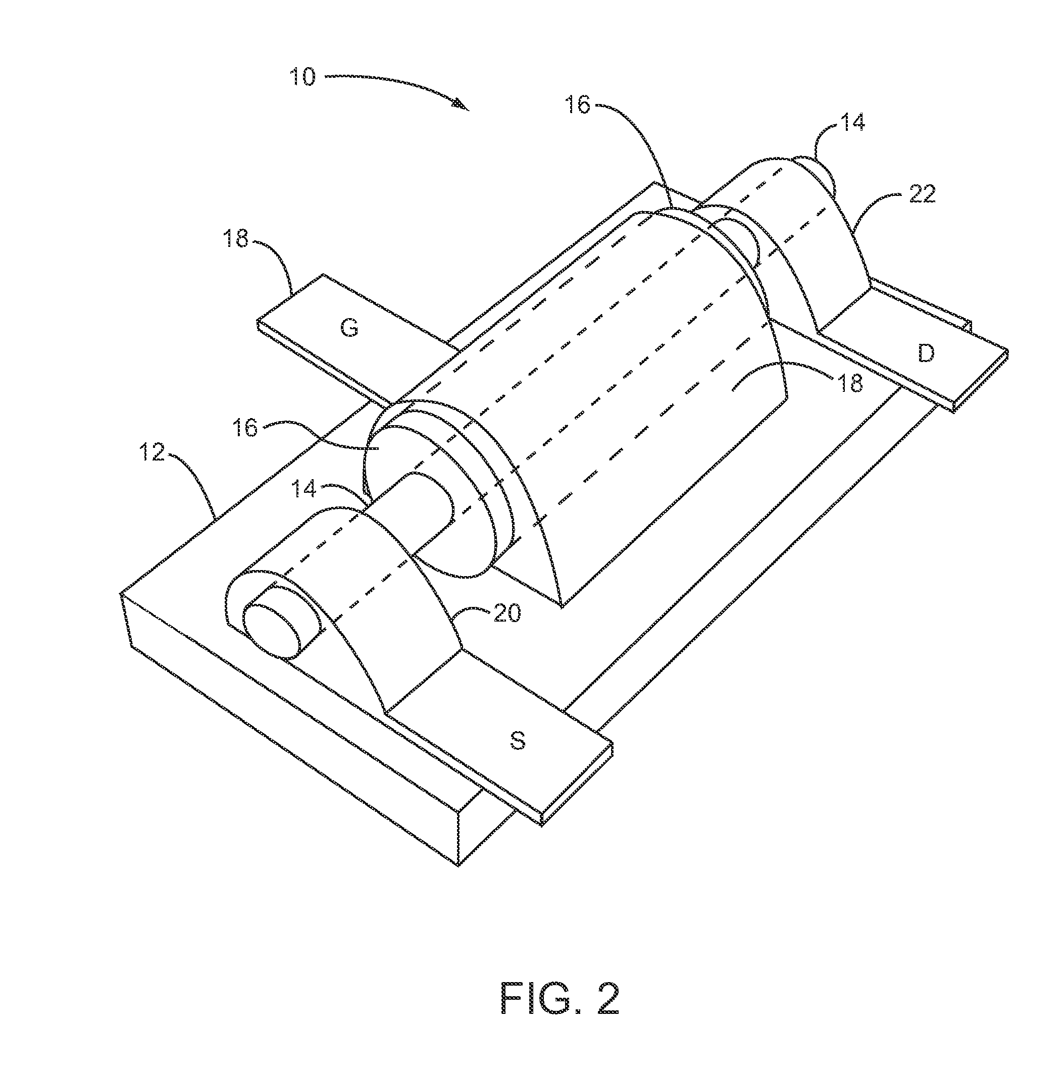
[0017]The crystal lattice of the material forming the channel of a transistor is formed from a moving atomic structure. The atoms of the crystal lattice vibrate as a function of temperature. These atoms will vibrate throughout normal operating temperature ranges of the transistor. The vibrating atoms are constantly changing the paths that are available for carriers, either electrons or holes, to flow through the crystal lattice of...


PUM


Abstract

The present invention provides a nanometer-scale transistor architecture providing enhanced carrier mobility. In particular, a portion of a channel of a transistor is substantially surrounded with an acoustically hard material to form a barrier shell about the channel. The barrier shell functions to confine phonons in the channel. Confining the phonons in the channel reduces the extent to which atoms in the crystal lattice structure of the channel move as they vibrate. Restricting the extent that the atoms vibrate in the crystal lattice of the channel significantly reduces the scattering of electrons or holes traveling through the channel. In one embodiment of the invention, the thickness of the channel is in the order of the thermal phonon wavelength of the material forming the channel, and the barrier shell is acoustically harder than the channel. The benefits of the present invention may be provided without requiring strain engineering.

Description

FIELD OF THE INVENTION[0001]The present invention relates to transistors, and in particular to nanometer-scale transistor architectures providing enhanced carrier mobility.BACKGROUND OF THE INVENTION[0002]Transistors, such as field effect transistors (FETs), have become ubiquitous in modern electronics and are employed to perform amplifier or switching functions in applications ranging from power amplifiers to digital processors. In many applications, either the need for additional functionality or miniaturization has led to aggressive downsizing of transistors. Unfortunately, the physical laws and material limits prevent continuous downsizing and require new approaches for increasing speed and functionality.[0003]In general, FETs rely on an electric field applied at a gate terminal to control the conductivity of a semiconductor channel extending between the source and drain terminals of the transistor. The electrical conductivity of the semiconductor channel corresponds to the rate...

Claims


Application Information

Patent Timeline
17 Jan 2012
Publication
US8097922B1
IPC
H01L21/70
CPC
H01L29/0673; H01L29/0676; H01L29/42392; H01L29/78696; H01L29/78642
Inventors
BALANDIN, ALEXANDER A.; FONOBEROV, VLADIMIR A.