CMOS variable gain amplifier

a variable gain amplifier and amplifier technology, applied in differential amplifiers, amplifiers with semiconductor devices/discharge tubes, amplifiers, etc., can solve the problems of limited gain variation range of variable gain amplifiers which may be used in agc devices, small integrated area, and difficulty in implementing devices with low power consumption

Active Publication Date: 2012-01-24
ELECTRONICS & TELECOMM RES INST
View PDF3 Cites 8 Cited by
  • Summary
  • Abstract
  • Description
  • Claims
  • Application Information

AI Technical Summary

Problems solved by technology

Therefore, the gain variation range of the variable gain amplifier which may be used in the AGC device is limited to a linear-in-dB gain period.
However, since a receiver of the communication system using the variable gain amplifier should additionally include the exponential signal converter configured to generate a linear-in-dB gain control signal in addition to the variable gain amplifier, it is difficult to implement a device having a low power consumption and a small integrated area.

Method used


Image

  • CMOS variable gain amplifier
  • CMOS variable gain amplifier
  • CMOS variable gain amplifier

Examples


Embodiment Construction

[0018]Exemplary embodiments of the present invention will be described below in more detail with reference to the accompanying drawings. The present invention may, however, be embodied in different forms and should not be constructed as limited to the embodiments set forth herein. Rather, these embodiments are provided so that this disclosure will be thorough and complete, and will fully convey the scope of the present invention to those skilled in the art. Throughout the disclosure, like reference numerals refer to like parts throughout the various figures and embodiments of the present invention.

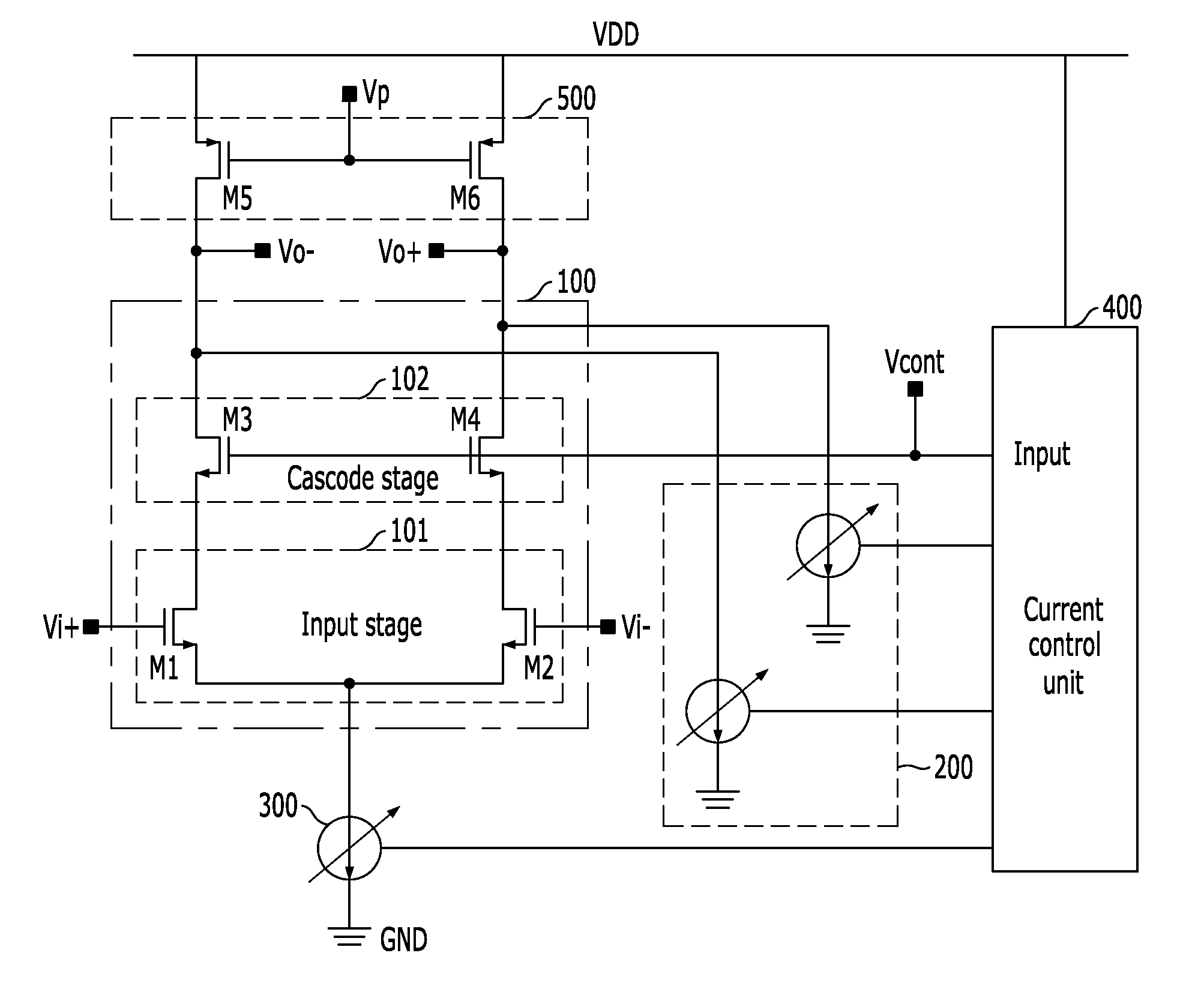
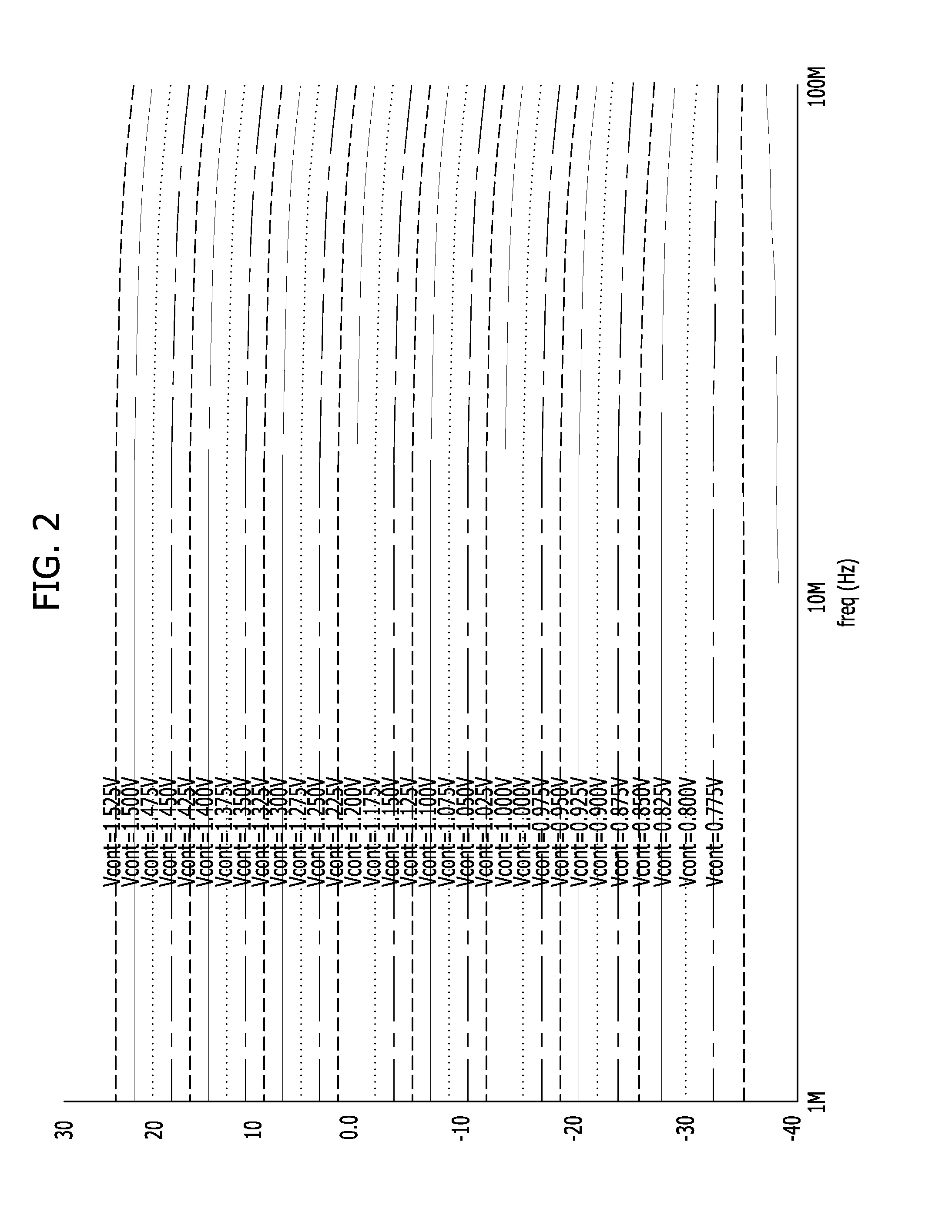
[0019]FIG. 1 is a circuit diagram illustrating a CMOS variable gain amplifier in accordance with an embodiment of the present invention. Referring to FIG. 1, the CMOS variable gain amplifier in accordance with the embodiment of the present invention includes a cascode amplifier 100, a first current generation unit 200, a second current generation unit 300, a current control unit 400, and a...


PUM


Abstract

A complementary metal-oxide semiconductor (CMOS) variable gain amplifier includes: a cascode amplifier including a common source field effect transistor and a common gate field effect transistor in a cascode structure; a first current generation unit connected in parallel to a drain of the common gate field effect transistor and configured to vary transconductance of the cascode amplifier; a second current generation unit connected to a common source of the cascode amplifier and configured to control a bias current of the cascode amplifier; a current control unit configured to generate a current control signal for the first and second current generation units; and a load stage connected in series to a drain of the cascode amplifier and configured to output an output current, which is varied by the overall transconductance of the cascode amplifier, as a differential output voltage.

Description

CROSS-REFERENCE(S) TO RELATED APPLICATIONS[0001]The present application claims priority of Korean Patent Application No. 10-2009-0086010, filed on Sep. 11, 2009, which is incorporated herein by reference in its entirety.BACKGROUND OF THE INVENTION[0002]1. Field of the Invention[0003]Exemplary embodiments of the present invention relate to a variable gain amplifier; and, more particularly, to a complementary metal-oxide semiconductor (CMOS) variable gain amplifier which has a wide linear-in-dB variable gain range to process an input signal having a wide range of magnitudes.[0004]2. Description of Related Art[0005]In a general communication system, a signal outputted from a transmitter is inputted to a receiver through a communication channel having various attenuation characteristics. At this time, in order to restore information transmitted from the transmitter from the inputted signal having a wide range of magnitudes, a process of controlling the inputted signal to a constant magn...

Claims


Application Information

Patent Timeline
Patent Type & Authority Patents(United States)
IPC IPC(8): H03F3/45
CPCH03F3/45188H03F3/4565H03G1/0029H03G7/001H03F2203/45074H03F2203/45414H03F2203/45302H03F2203/45082H03G3/30
Inventor JANG, SEUNGHYUNLEE, KWANG-CHUN
Owner ELECTRONICS & TELECOMM RES INST
Why Eureka
Try Eureka