High efficiency optical mode transformer for matching a single mode fiber to a high index contrast planar waveguide

a high-efficiency, planar waveguide technology, applied in the direction of optical waveguide light guide, optical elements, instruments, etc., can solve the problems of not being able to achieve mode transformation to or from a high index difference waveguide, not being able to perform lithographic processes in time, and not being able to control etching techniques and therefore difficult to manufactur

Active Publication Date: 2012-02-14
INFINERA CORP
View PDF12 Cites 24 Cited by
  • Summary
  • Abstract
  • Description
  • Claims
  • Application Information

AI Technical Summary

Problems solved by technology

Vertical tapering uses special etching techniques that are not well controlled and therefore difficult to manufacture.
This is not a suitable method for mode transformation to or from a high index difference waveguide.
also come down to a sharp point, which makes it almost impossible to perform in a lithographic process.
In constructing integrated optical circuits, space constraints and the desire to operate on multiple input waveguides often necessitate waveguide crossings.
Any additional three-dimensional structure adds considerable manufacturing difficulty.
However, it requires an additional step of etching and epitaxially regrowth, thus giving rise to an increase in the cost price of the component.
Although the technique of butt coupling is well mastered, it remains a difficult and extremely important step.
This method is relatively complex to implement and entails costs that are still high.
However, it cannot be used to optimize the two waveguides, namely the active waveguide and the passive waveguide, separately.
This means that it necessitates compromises.
Furthermore, this method does not enable a clear definition of the boundary between the two types of guides, active and passive, because the change in state is gradual.
The fact of not being able to define this boundary causes penalties because it is difficult to know where to position the electrode necessary for the operation of the component.
By contrast, if it covers a part of the passive guide, electrical leaks are created that penalize and degrade the threshold current, efficiency current and efficiency parameters.
None of the prior art provides for an efficient mode transformation between a low index difference and a high index difference waveguide on a microchip.

Method used


Image

  • High efficiency optical mode transformer for matching a single mode fiber to a high index contrast planar waveguide
  • High efficiency optical mode transformer for matching a single mode fiber to a high index contrast planar waveguide
  • High efficiency optical mode transformer for matching a single mode fiber to a high index contrast planar waveguide

Examples


Embodiment Construction

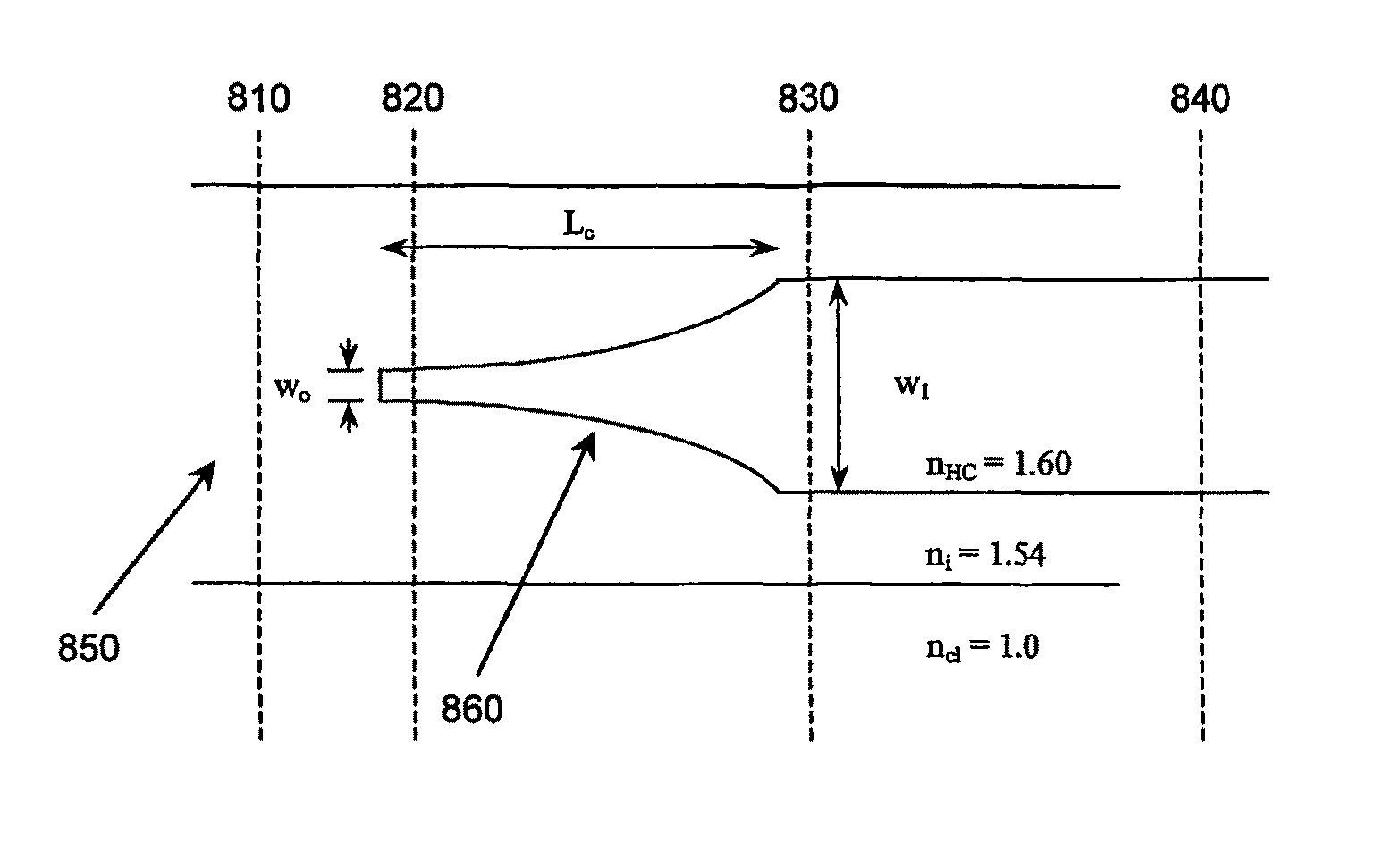
[0043]The following description will further help to explain the inventive features of the High Efficiency Optical Mode Transformer for Matching a Single Mode Fiber with a High-Index Contrast Planar Waveguide on a microchip.

[0044]The approach used in this invention is to separate the problem into two steps with definitive objectives. The first objective is to get optical power from the SM fiber onto the chip (but not into the HC guide) with the highest possible efficiency. Once high efficiency connectivity and optical power transmission is established onto the chip, power is then transferred into the HC waveguide via an on chip mode transformer.

[0045]A large planar waveguide is fabricated on the chip for the purpose of obtaining maximum coupling efficiency from a fiber to a specific structure on the chip. The dimensions of the large waveguide are chosen so as to achieve maximum coupling efficiency. This waveguide is referred to as a fiber-matched waveguide. An optical mode transform...


PUM


Abstract

The present invention includes a device and a method for fabricating a device that is an optical power mode transformer that accepts light in a mode transformation direction where the transformer is attached to or embedded in a semiconductor microchip and includes a first single or multimode optical input (SM) waveguide including a first core surrounded by a cladding, and, a second high contrast index grade (HC) waveguide including a second core having a tapered region and surrounded by said cladding, a portion of the tapered region of the core being embedded within the first optical input waveguide region with an embedded length sufficient for efficient light transfer from the first input waveguide to the said second waveguide wherein the embedded portion of the tapered region is fully surrounded by the first input waveguide along an axial and radial cross-section of the second waveguide in the mode transformation direction. In this manner, it is possible that the long (SM) waveguide eventually actually acts as a cladding for the (HC) waveguide.

Description

CLAIM TO PRIORITY[0001]Applicants hereby claim priority under all rights to which they are entitled under 35 U.S.C. Section 119 based upon the Provisional Application Ser. No. 60 / 280,935 for this Patent Cooperation Treaty (PCT) patent application (USPTO receiving office) filed at the United States Patent and Trademark Office on Apr. 3, 2001.FIELD OF INVENTION[0002]This invention relates to the transferal of optical power from a single mode (SM) optical fiber into a much smaller, high-index contrast (HC) waveguide. HC waveguides are desirable for making ultra-compact optical circuits on a semiconductor or dielectric microchip. These waveguides consist of cross-sectional dimensions that are much smaller than conventional SM fibers. Directly connecting a SM fiber to a HC waveguide is quite impractical, as the result would be poor or insufficient optical power transfer. This optical power transfer is more commonly described as coupling efficiency. To efficiently couple two waveguides wi...

Claims


Application Information

Patent Timeline
Patent Type & Authority Patents(United States)
IPC IPC(8): G02B6/26H04B10/00G02B6/122G02B6/30
CPCG02B6/1228G02B6/305
Inventor LITTLE, BRENT E.CHU, SAITAK
Owner INFINERA CORP
Why Eureka
Try Eureka