

Surface plasmon polariton waveguide
A surface plasmon and waveguide technology, applied in the field of waveguides, can solve the problems of increased loss, difficult loss of propagation length, etc., to achieve the effects of improving efficiency, enhancing mode locality, and improving energy density
- Summary
- Abstract
- Description
- Claims
- Application Information
AI Technical Summary
Problems solved by technology
Method used
Image

Examples
Embodiment Construction
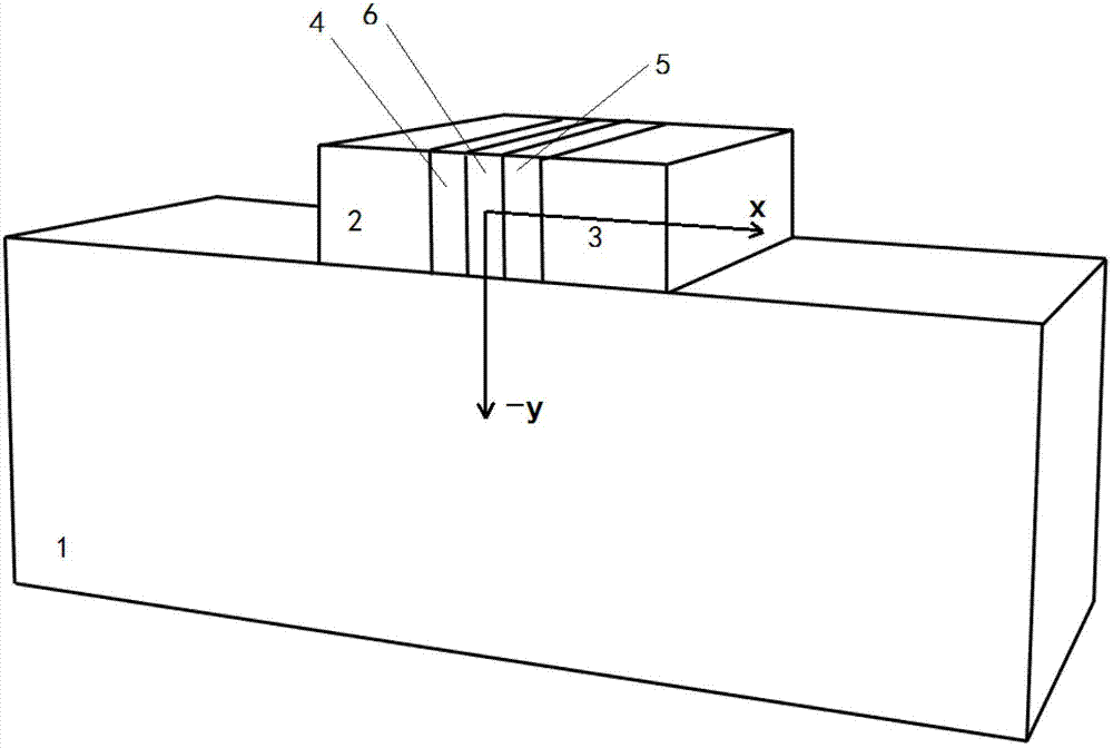
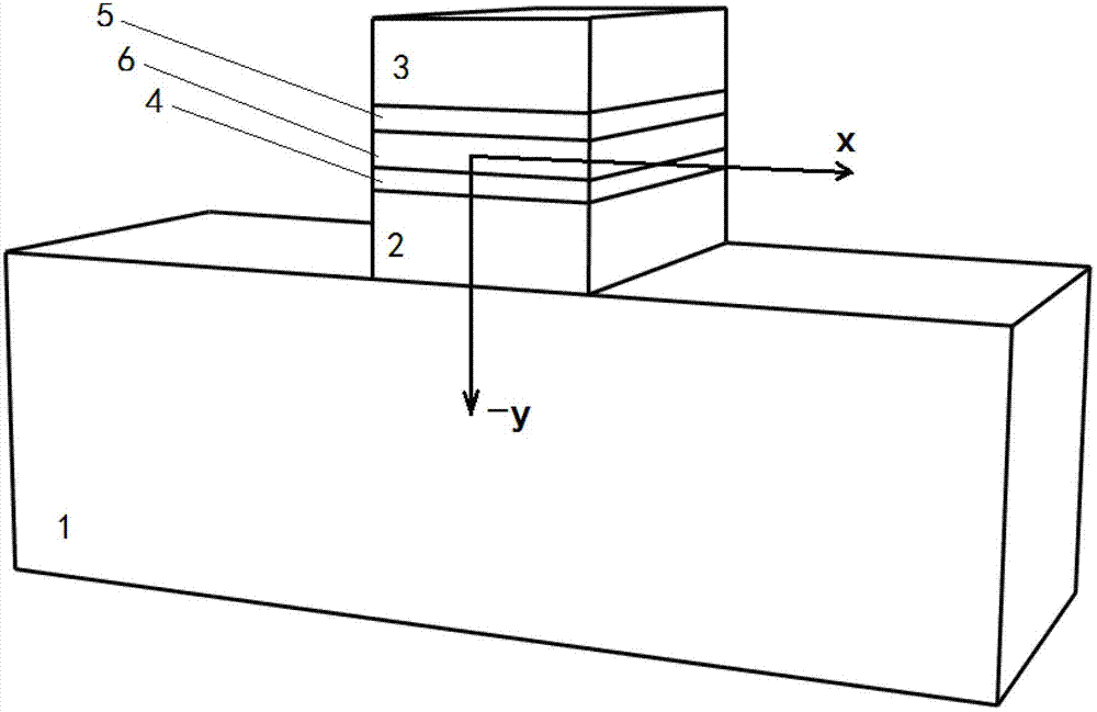
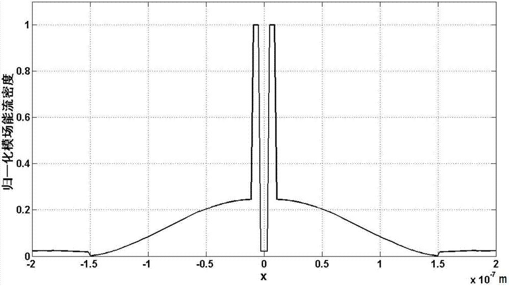
[0017] The invention provides a hybrid surface plasmon slot waveguide, which is specifically represented by adding metal materials in the slot region on the basis of the commonly used slot waveguide, thereby obtaining a novel hybrid surface plasmon waveguide with enhanced mode field confinement. The waveguide mode in the slot can be regarded as a hybrid of the traditional slot waveguide mode and the metal-dielectric surface plasmon waveguide mode. The low-refractive-index dielectric slot region of the traditional slotted waveguide is changed to a sandwich structure: a distribution of "low-refractive-index dielectric-metal-low-refractive-index dielectric". The mode field can be well confined in the two low index dielectric layers on either side of the metal in the sandwich. The resulting hybrid mode has the dual characteristics of low loss in the slot waveguide mode and good mode field confinement in the metal-dielectric surface plasmon mode, so that the waveguide region has a ...
PUM
| Property | Measurement | Unit |
|---|---|---|
| Length | aaaaa | aaaaa |
Abstract
Description
Claims
Application Information