Deep ultraviolet micro-LED with high electro-optical conversion rate and inverted structure and preparation method of deep ultraviolet micro-LED

An electro-optical conversion and deep ultraviolet technology, which is applied in the direction of circuits, electrical components, semiconductor devices, etc., can solve the problems of sudden drop in light extraction efficiency, difficulties in light extraction efficiency, and inability to achieve large-scale commercialization and practical application, and achieve improvement Light extraction efficiency and anti-static breakdown ability, reducing forward conduction voltage and reverse leakage current, and improving device performance

Active Publication Date: 2021-03-23
PEKING UNIV
View PDF9 Cites 7 Cited by
  • Summary
  • Abstract
  • Description
  • Claims
  • Application Information

AI Technical Summary

Problems solved by technology

However, the light extraction efficiency (LEE) of deep ultraviolet (DUV LEDs) is difficult to exceed 10%, and the technical indicators for large-scale commercialization and practicality cannot be achieved.
One of the main reasons for such a low LEE is that when the emission wavelength is lower than 280nm, the light output mode of the UV LED changes from the

Method used


Image

  • Deep ultraviolet micro-LED with high electro-optical conversion rate and inverted structure and preparation method of deep ultraviolet micro-LED
  • Deep ultraviolet micro-LED with high electro-optical conversion rate and inverted structure and preparation method of deep ultraviolet micro-LED
  • Deep ultraviolet micro-LED with high electro-optical conversion rate and inverted structure and preparation method of deep ultraviolet micro-LED

Examples


Embodiment 1

[0047] This embodiment is a method for preparing a chip unit with a 222 nm light emission wavelength in TM mode. The method for preparing a deep ultraviolet micro-LED with a high electrical-to-optical conversion rate flip-chip structure in this embodiment includes the following steps:

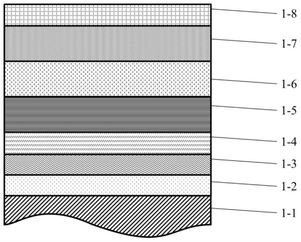
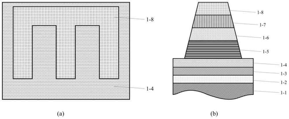
[0048] 1) Select a nitride semiconductor LED epitaxial wafer. From bottom to top, the semiconductor LED epitaxial wafer is the substrate 1-1 using sapphire, the nucleation layer 1-2 using AlN, the buffer layer 1-3 using AlGaN, and the N of AlGaN. Type doped layer 1-4, AlGaN / AlGaN multiple quantum well active region 1-5, electron blocking layer 1-6 and P-type doped layer composed of AlGaN 1-7 and GaN 1-8 The LED epitaxial wafer is pretreated to make the surface clean, such as figure 1 shown;

[0049] 2) According to the requirements of the prepared micro-LED, design an exposure layout with a size of 50 μm in length and 50 μm in width; spin-coat positive photoresist on the upper surface of the P...

Embodiment 2

[0059] This embodiment is a method for preparing a plurality of chip units with an emission wavelength of 278 nm. The method for preparing a deep-UV micro-LED with a high electro-optical conversion rate flip-chip structure in this embodiment includes the following steps:

[0060] 1) Select a nitride semiconductor LED epitaxial wafer. From bottom to top, the semiconductor LED epitaxial wafer is the substrate 1-1 using sapphire, the nucleation layer 1-2 using AlN, the buffer layer 1-3 using AlGaN, and the N of AlGaN. Type doped layer 1-4, AlGaN / AlGaN multiple quantum well active region 1-5, electron blocking layer 1-6 and P-type doped layer composed of AlGaN 1-7 and GaN 1-8 The LED epitaxial wafer is pretreated to make the surface clean;

[0061] 2) According to the requirements of the prepared micro-LED, design the exposure layout, including a plurality of micro-mesa units, each of which is 25 μm long and 25 μm wide; spin-coat positive light on the upper surface of the P-type d...


PUM


Abstract

The invention discloses a high-reflectivity deep ultraviolet micro-LED with an inverted structure and a preparation method of the deep ultraviolet micro-LED. P-type ohmic contact metal is etched, thereserved P-type ohmic contact metal is a two-dimensional array composed of a plurality of small pattern units arranged periodically, a micro-grid P-type ohmic contact electrode is formed, Al metal isdeposited on the micro-grid P-type ohmic contact electrode, a reflecting layer is formed to cover a micro-mesa, the Al metal is completely embedded into a gap of the micro-grid P-type ohmic contact electrode, and the inclination angle of the side wall of the micro-mesa is adjusted between 30 degrees and 90 degrees. According to the invention, the micro-grid P-type ohmic contact electrode is adopted, the absorption loss of ultraviolet light in the LED structure is reduced, and the reflection of the ultraviolet light at the electrode is enhanced by the Al metal, so that most of emergent light isemitted from the back surface of the inverted structure, and the light extraction efficiency of the ultraviolet light in the UV LED is greatly improved; and the deep ultraviolet micro-LED is high inflexibility, is compatible with in-plane and vertical-structure inverted micro-LEDs, mini-LEDs and the like, facilitates the improvement of the performance of a device, and achieves the batch production.

Description

technical field [0001] The invention relates to the preparation technology of LED components, in particular to a deep-ultraviolet micro-LED with a high electro-optical conversion rate flip-chip structure and a preparation method thereof. Background technique [0002] Compared with traditional mercury lamps, AlGaN-based ultraviolet light-emitting diodes (UV LEDs) have many advantages, such as miniaturization, energy saving, environmental friendliness, and easy integration. With the continuous development of material epitaxy technology, the quality of AlGaN crystal has been continuously improved, so that the internal quantum efficiency (IQE) of UV LED has exceeded 60%. However, the light extraction efficiency (LEE) of deep ultraviolet (DUV LEDs) is difficult to exceed 10%, and cannot reach the technical indicators of large-scale commercialization and practicality. One of the main reasons for such a low LEE is that when the emission wavelength is lower than 280nm, the UV LED l...

Claims


Application Information

Patent Timeline
IPC IPC(8): H01L33/36H01L33/32H01L33/38H01L33/40H01L33/00
CPCH01L33/36H01L33/38H01L33/40H01L33/405H01L33/32H01L33/005Y02P70/50
Inventor 王新强李铎孙明刘权锋刘上锋康俊杰袁冶张国义
Owner PEKING UNIV
Why Eureka
Try Eureka