Novel fully passivated contact crystalline silicon solar cell and preparation method thereof

A technology for solar cells and crystalline silicon, applied in the field of solar cells, can solve the problems of large parasitic optical absorption loss, large resistivity of hydrogenated microcrystalline silicon oxide, etc.

Inactive Publication Date: 2019-08-09
ZHEJIANG NORMAL UNIVERSITY
View PDF4 Cites 8 Cited by
  • Summary
  • Abstract
  • Description
  • Claims
  • Application Information

AI Technical Summary

Problems solved by technology

However, SiO x The disadvantage of the /poly-Si passivation contact is that polysilicon has a band gap similar to that of crystalline silicon, and when this passivation structure is applied to the front side of the cell, it will generate large p

Method used


Image

  • Novel fully passivated contact crystalline silicon solar cell and preparation method thereof

Examples


Embodiment Construction

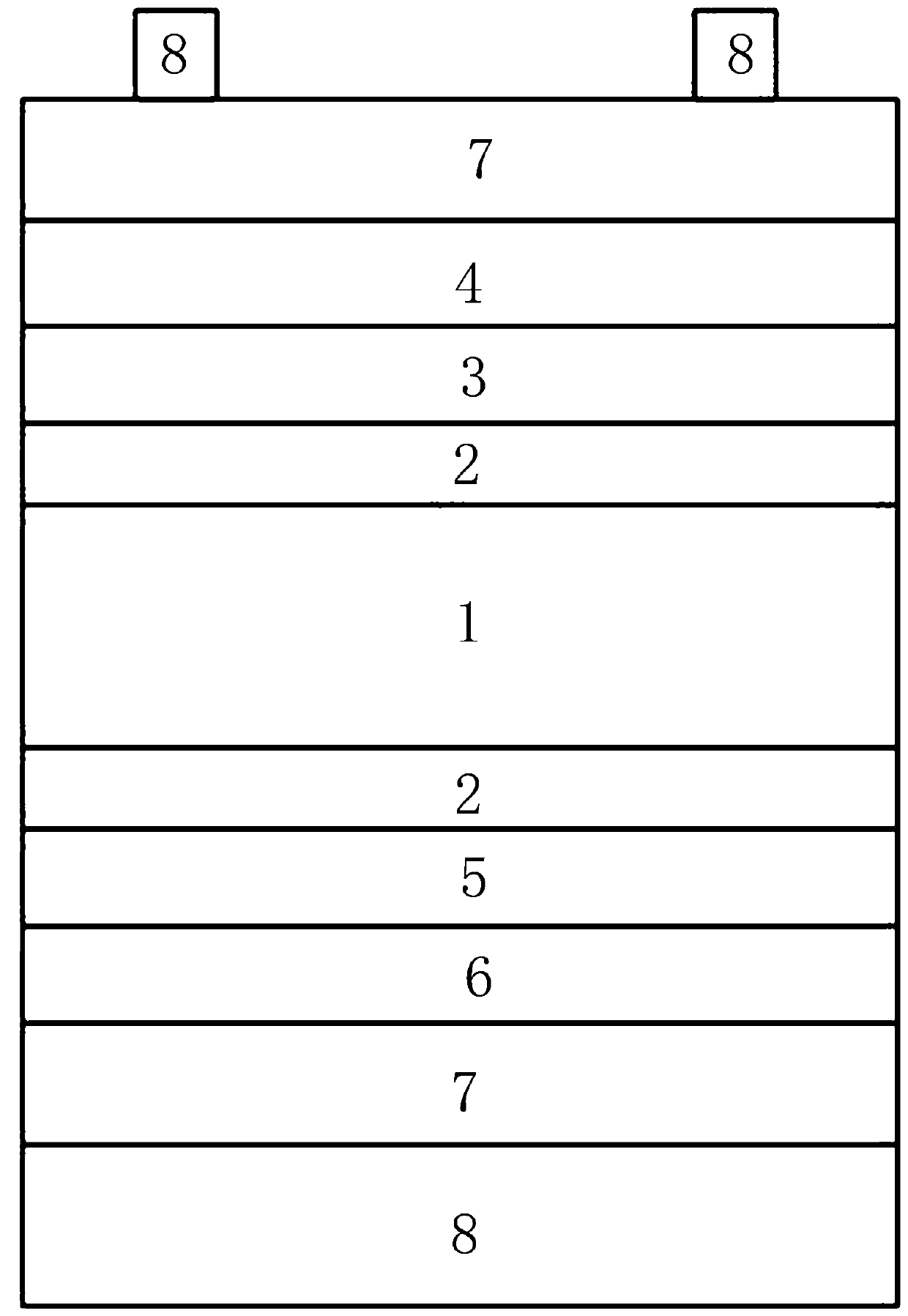
[0017] See attached picture. The solar cell described in this embodiment comprises a crystalline silicon layer 1 with an ultra-thin silicon oxide passivation layer 2 (1.4nm) on both sides, and a hydrogenated microcrystalline silicon oxide layer 3 (15nm) is grown sequentially on the front side of the silicon wafer , hydrogenated nanocrystalline silicon layer 4 (15nm), the two form a mixed-phase silicon oxide / nanocrystalline silicon layer; the reverse side also has intrinsic hydrogenated amorphous silicon layer 5 (10nm), p-type hydrogenated amorphous silicon layer 6 (10nm) , there are ITO layers 7 and Ag electrodes 8 on both sides.

[0018] When preparing:

[0019] 1. Silicon wafer cleaning and surface ultra-thin silicon oxide passivation layer growth

[0020] First, clean the silicon wafer and passivate the ultra-thin oxide layer, which can reduce the impurity concentration on the surface of the silicon wafer and reduce the interface defect state density between the silicon w...


PUM


Abstract

The invention discloses a novel fully passivated contact crystalline silicon solar cell and a preparation method thereof. The novel fully passivated contact crystalline silicon solar cell comprises acrystalline silicon layer, an ultra-thin silicon oxide passivation layer is arranged on the two sides, a mixed phase silicon oxide/nanocrystalline silicon layer is arranged on the front surface, an intrinsic hydrogenated amorphous silicon layer and a p-type hydrogenated amorphous silicon layer are arranged on the reverse surafce, and an ITO layer and an Ag electrode are arranged outside the two sides. The mp-SiOx/nc-Si is applied to replace the poly-Si layer in the SiOx/poly-Si passivation contact structure of the TOPCon cell to act as the front passivation contact of the cell, and the intrinsic hydrogenated amorphous silicon (a-Si: H (i)) and the doped a-Si: H stack layer are used as the reverse passivation contact and the fully passivated contact crystalline silicon solar cell is designed and prepared so that the electrical and optical properties of the front surface of the passivated contact crystalline silicon solar cell can be enhanced.

Description

technical field [0001] The invention belongs to the technical field of solar cells, in particular to a novel fully passivated contact crystalline silicon solar cell and a preparation method thereof. Background technique [0002] The key factor limiting the further improvement of the efficiency of traditional crystalline silicon (c-Si) solar cells is the carrier recombination loss at the contact interface between metal electrodes and silicon. The traditional way to solve this problem is to use local contact, such as Emitter and Rear Surface Passivation Cell (PERC), Emitter Passivation and Rear Partial Diffusion Cell (PERL), etc. However, these localized contact structures increase the complexity of the battery process while making lateral transport a key factor in battery design. Specifically, there is a trade-off between open-circuit voltage and fill factor due to increased ohmic contact losses due to lateral carrier transport. Another method to reduce contact recombinat...

Claims


Application Information

Patent Timeline
IPC IPC(8): H01L31/0216H01L31/0336H01L31/074H01L31/18
CPCH01L31/02167H01L31/0336H01L31/074H01L31/1868Y02E10/50Y02P70/50
Inventor 黄仕华周理想池丹丁月珂芮哲
Owner ZHEJIANG NORMAL UNIVERSITY
Why Eureka
Try Eureka