Hybrid nanotube/CMOS dynamically reconfigurable architecture and an integrated design optimization method and system therefor

a nanotube/cmos, dynamic reconfigurable technology, applied in the direction of computation using denominational number representation, pulse technique, instruments, etc., to achieve the effect of improving area/executive time features

Inactive Publication Date: 2012-02-14
QUEENS UNIV OF KINGSTON +1
View PDF130 Cites 12 Cited by
  • Summary
  • Abstract
  • Description
  • Claims
  • Application Information

AI Technical Summary

Benefits of technology

[0008]The logic implemented in the logic elements of the reconfigurable architecture of the present invention can be changed every few cycles, making both coarse-grain and fine-grain dynamic reconfiguration possible. The present invention thereby addresses two primary challenges in existing CMOS-based FPGAs: logic density and efficiency of run-time reconfiguration. Traditional reconfigurable architectures only allow partial dynamic reconfiguration, (i.e., only a part of the architecture can be reconfigured at run-time) due to the area overhead associated with SRAMs that store the reconfiguration bits and the long latency of reconfiguration due to the accessing of off-chip storage. Since the access latency of on-chip storage is small, on-chip storage provides an opportunity to store multiple logic designs in the on-chip storage, and to invoke different designs through fine-grain dynamic reconfiguration.
[0021]reduce by 50% or more a need for deep interconnect hierarchy when using level-1 folding;

Problems solved by technology

Traditional reconfigurable architectures only allow partial dynamic reconfiguration, (i.e., only a part of the architecture can be reconfigured at run-time) due to the area overhead associated with SRAMs that store the reconfiguration bits and the long latency of reconfiguration due to the accessing of off-chip storage.

Method used


Image

  • Hybrid nanotube/CMOS dynamically reconfigurable architecture and an integrated design optimization method and system therefor
  • Hybrid nanotube/CMOS dynamically reconfigurable architecture and an integrated design optimization method and system therefor
  • Hybrid nanotube/CMOS dynamically reconfigurable architecture and an integrated design optimization method and system therefor

Examples


Embodiment Construction

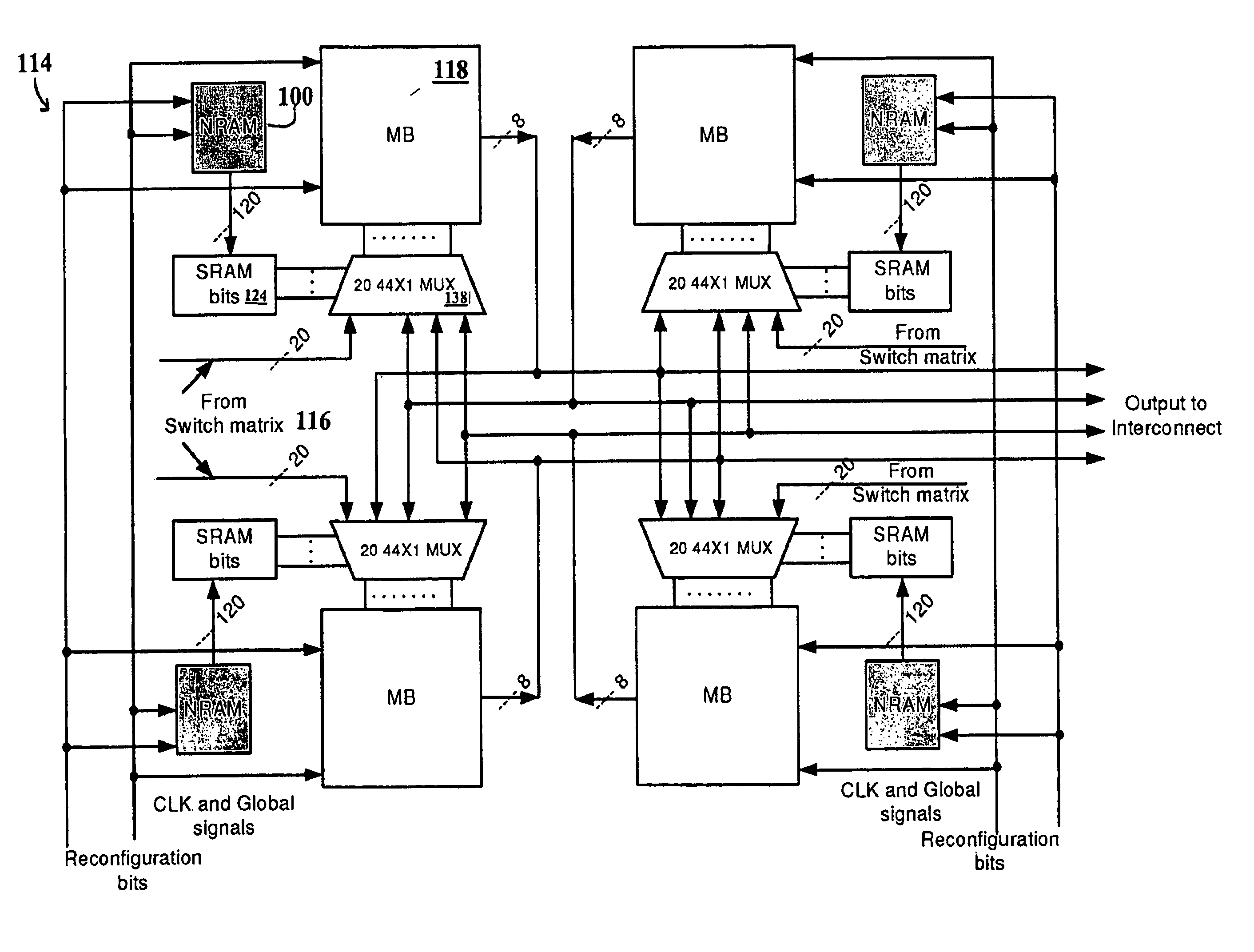
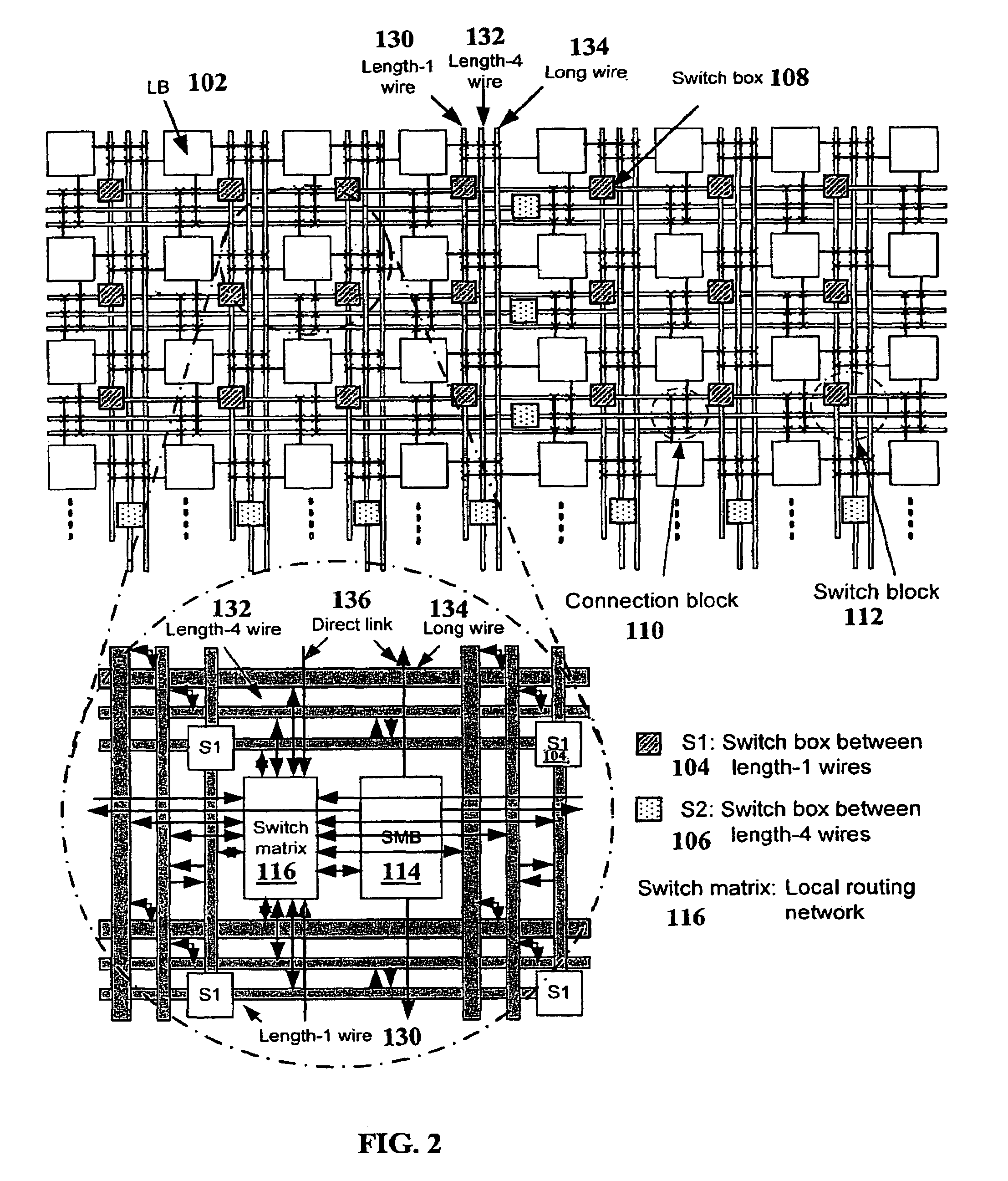
[0057]A high-performance run-time reconfigurable architecture is provided, along with a design optimization method and system to efficiency balance performance and area considerations of the architecture. A high-density, high-speed non-volatile memory is implemented in the architecture to enable cycle-by-cycle reconfiguration and logic folding. Choice of different folding levels allows the designer flexibility in performing area-performance trade-offs. The significant increase in relative logic density (more than an order of magnitude for larger circuits) made possible by the present invention can allow the use of cheaper reconfigurable architectures with smaller logic capacities to implement the same functionality, thus giving a boost to such use in cost-conscious embedded systems.

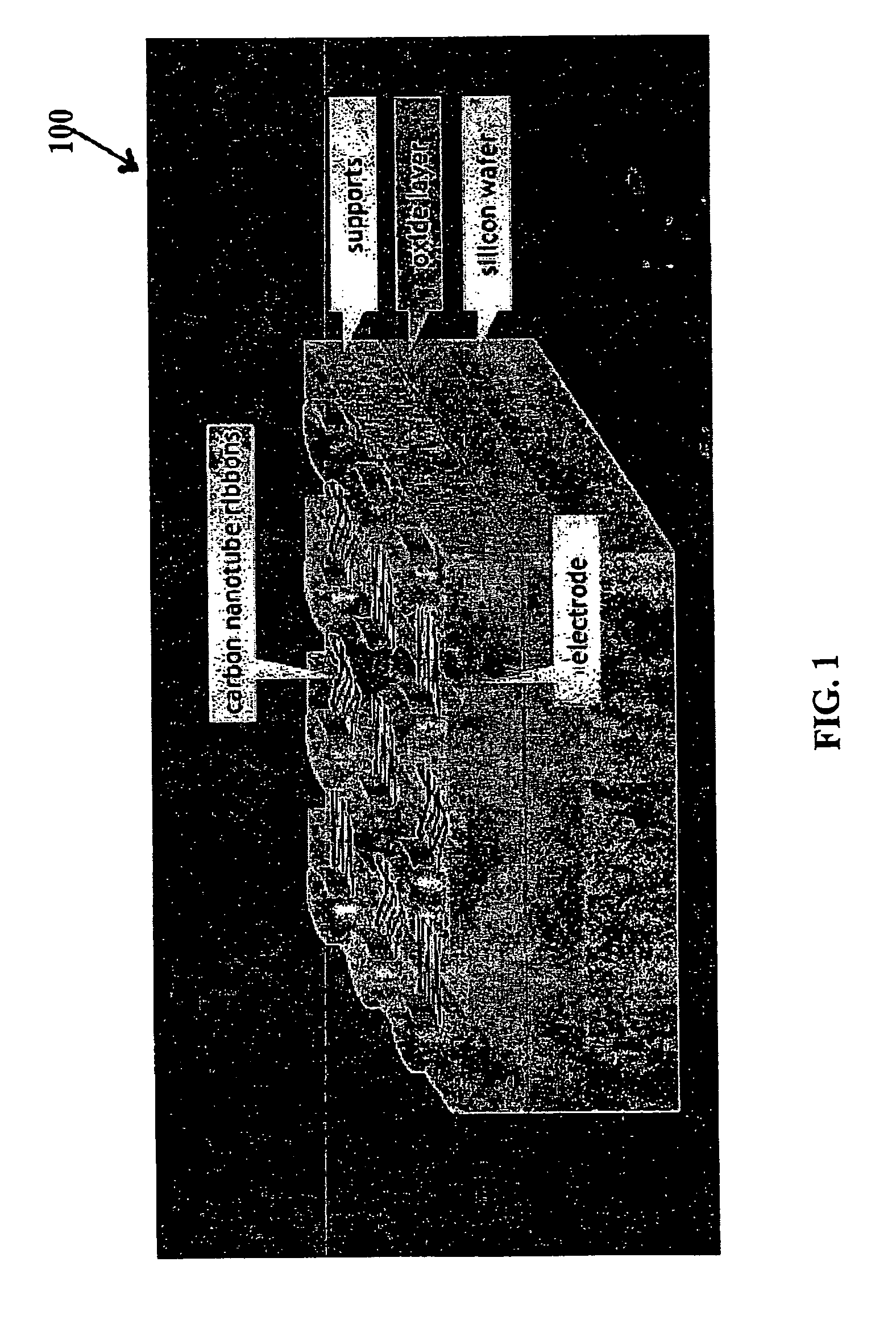
[0058]One embodiment of the invention implements a non-volatile nanotube random-access memory, that is considerably faster and denser than DRAM, has much lower power consumption than DRAM or flash, has si...


PUM


Abstract

A hybrid nanotube, high-performance, dynamically reconfigurable architecture, NATURE, is provided, and a design optimization flow method and system, NanoMap. A run-time reconfigurable architecture is provided by associating a non-volatile universal memory to each logic element to enable cycle-by-cycle reconfiguration and logic folding, while remaining CMOS compatible. Through logic folding, significant logic density improvement and flexibility in performing area-delay tradeoffs are possible. NanoMap incorporates temporal logic folding during the logic mapping, temporal clustering and placement steps. NanoMap provides for automatic selection of a best folding level, and uses force-direct scheduling to balance resources across folding stages. Mapping can thereby target various optimization objectives and user constraints. A high-density, high-speed carbon nanotube RAM can be implemented as the universal memory, allowing on-chip multi-context configuration storage, enabling fine-grain temporal logic folding, and providing a significant increase in relative logic density.

Description

RELATED APPLICATIONS[0001]This application is a 371 application of International Application No. PCT / US2007 / 009658 filed Apr. 19, 2007, which claims benefit of U.S. Provisional Application Ser. Nos. 60 / 793,665, filed Apr. 19, 2006, entitled “A Hybrid Nanotube / CMOS Dynamically Reconfigurable Architecture;” and 60 / 919,225, filed Mar. 21, 2007, entitled “NanoMap: An Integrated Design Optimization Flow for a Hybrid Nanotube / CMOS Dynamically Reconfigurable Architecture.” Each of the above-identified related applications are incorporated herein by this reference.GOVERNMENT RIGHTS[0002]This invention was made with government support under Grant #CCF-0429745 awarded by the National Science Foundation. The Government has certain rights in the invention.FIELD OF THE INVENTION[0003]This invention relates generally to reconfigurable computer architectures, and particularly to CMOS compatible field-programmable gate arrays (FPGAs) having non-volatile universal memories supporting fine-grain reco...

Claims


Application Information

Patent Timeline
Patent Type & Authority Patents(United States)
IPC IPC(8): G06F1/24
CPCH03K19/17752G11C11/40615H03K19/1778H03K19/17776H01L51/0052H03K19/17758H10K85/615
Inventor ZHANG, WEIJHA, NIRAJ K.SHANG, LI
Owner QUEENS UNIV OF KINGSTON
Why Eureka
Try Eureka