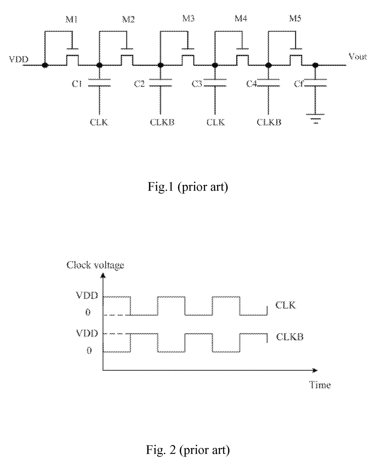
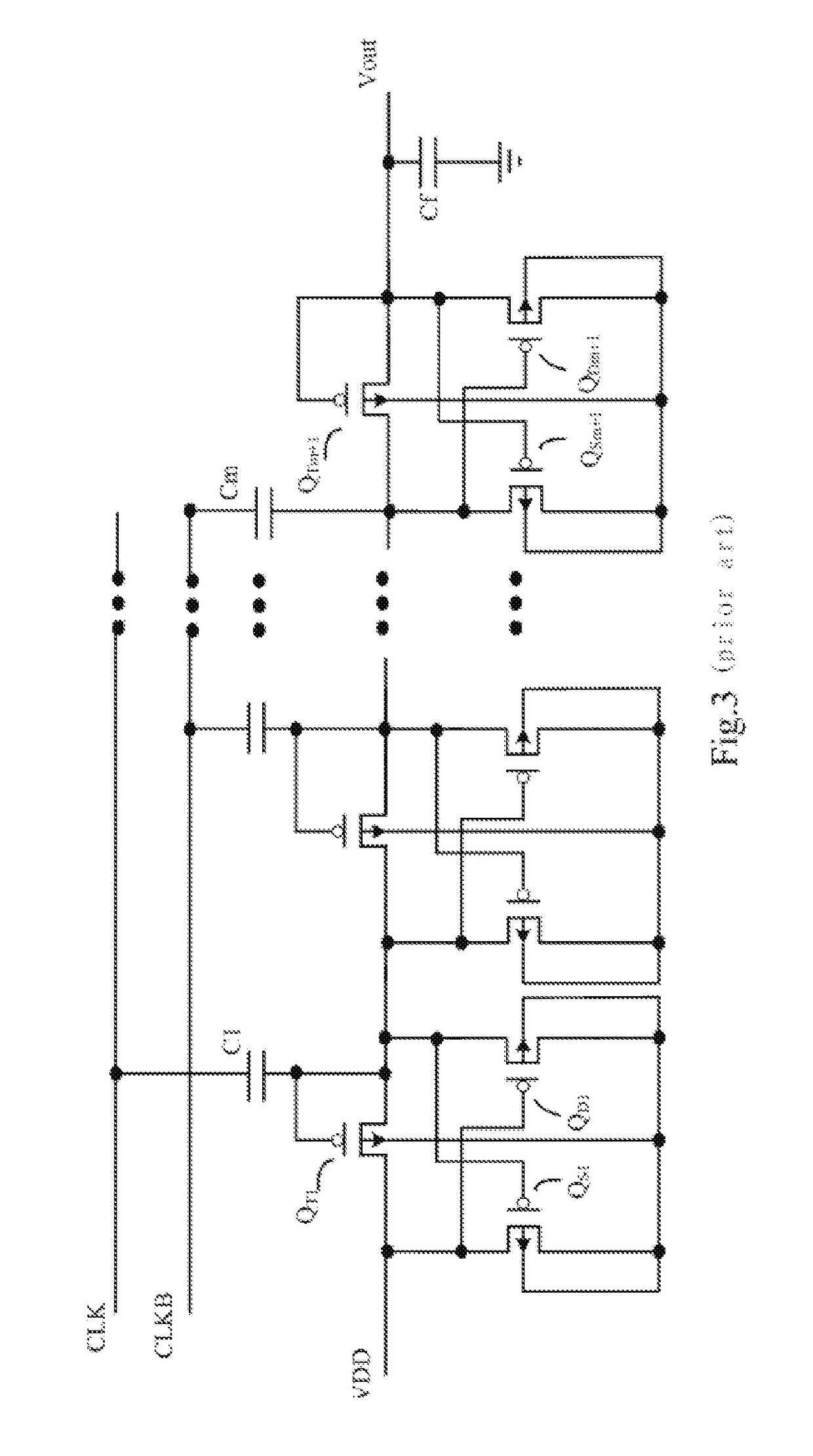
Charge pump circuit

a charge pump and circuit technology, applied in the direction of power conversion systems, instruments, dc-dc conversion, etc., can solve the problems of reducing the voltage gain affecting the efficiency of boosting the voltage through the charge pump, and reducing the transmission efficiency of the charge pump circuit. , to achieve the effect of reducing the transmission efficiency

Active Publication Date: 2012-02-21
SEMICONDUCTOR MANUFACTURING INTERNATIONAL (BEIJING) CORP
View PDF9 Cites 12 Cited by
  • Summary
  • Abstract
  • Description
  • Claims
  • Application Information

AI Technical Summary

Benefits of technology

[0036]Optionally, the switch unit further includes a substrate bias unit in correspondence with the PMOS transistor in the switch unit and adapted to avoid presence of leakage current in the corresponding PMOS transistor.
[0038]As compared with the prior art, the embodiment of the invention adopts the first NMOS transistor and at least one PMOS transistor as the switch unit during transmission and thus can address effectively the problem that the all-NMOS transistor circuit may have degraded transmission efficiency and even can not work because the threshold voltage of the NMOS transistor increases due to the body effect in the circuit, and also can ensure that the respective MOS transistors will be provided with a high turn-on voltage, for example, two times the input voltage VDD, and thus the circuit can still work normally even in the case of a low input voltage VDD.

Problems solved by technology

In the above circuit, each NMOS transistor with the gate and the source in connection may give rise to a loss of threshold voltage, and this may reduce the voltage gain of the charge pump circuit, lower transmission efficiency of the charge pump circuit and further increase area of the circuit.
Also each stage of transmission unit may be insufficiently turned on along with the steadily lowered VDD, thereby influencing the efficiency of boosting the voltage through the charge pump.
Even if the minimum gate-source voltage required for turning on each NMOS transistor differs and although several preceding NMOS transistors can be turned on thoroughly, the turn-on of the NMOS transistors may become more and more insufficient and seriously even an NMOS transistor in a transmission unit may fail to be turned on along with the increment of the numbers of transistors, thereby influencing normal work of the entire circuit.
However, this structure can not ensure sufficient turn-on of the PMOS transistors in all the transmission units in the case of a low input voltage VDD and may be inefficient with boosting the voltage at each stage.
The inefficiency of transferring may require a circuit with a larger number of stages, thereby resulting in a slowed processing speed, more noise and an increased chip area of the circuit.

Method used


Image

  • Charge pump circuit
  • Charge pump circuit
  • Charge pump circuit

Examples


first embodiment

The First Embodiment

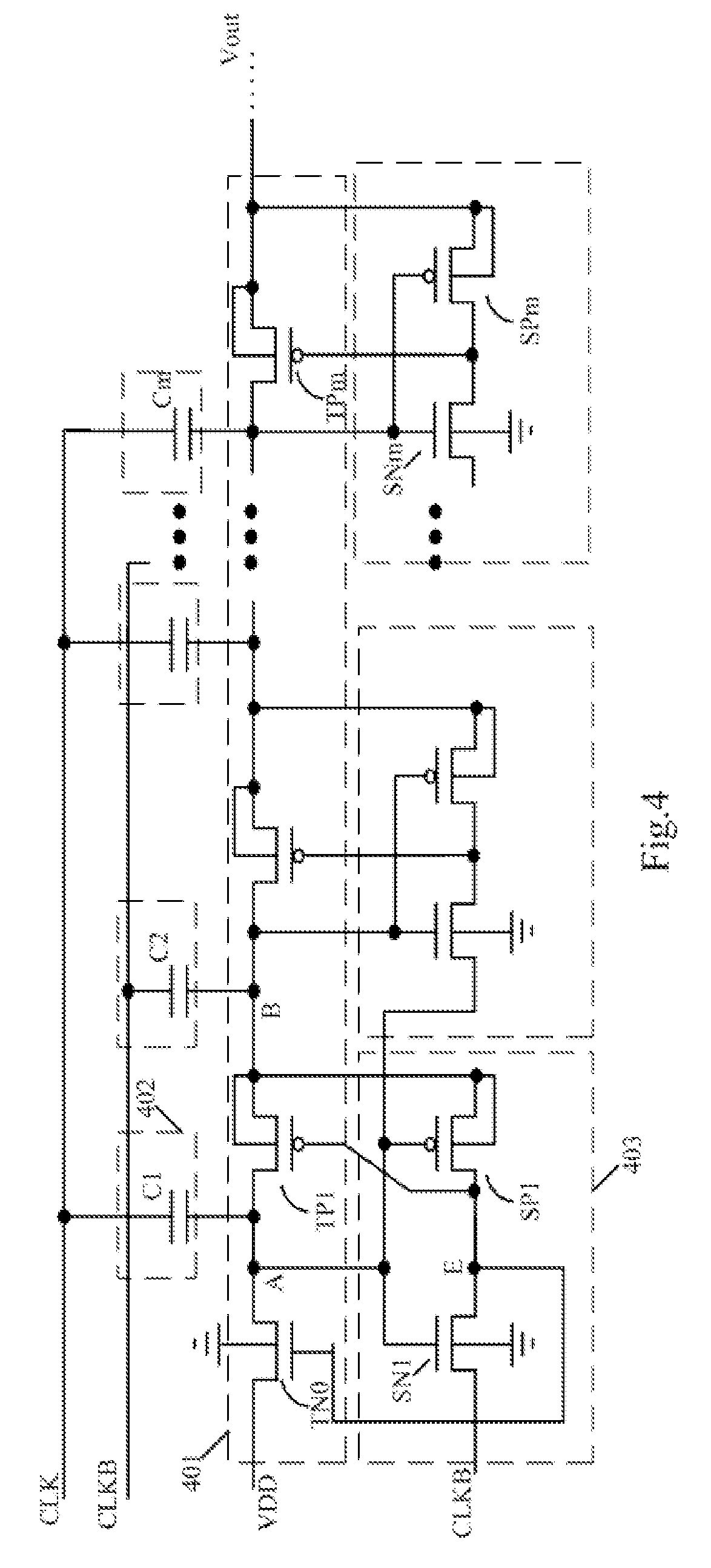
[0066]Referring to FIG. 4, an embodiment of the invention provides a charge pump circuit including: a switch unit 410 including a first NMOS transistor TN0 and m PMOS transistors TPi (in which, 1≦i≦m, m≧1); m stages of charging units each including a charging capacitor Ci; and a transmission unit including m stages of transmission sub-units each including an NMOS transistor and a PMOS transistor.

[0067]In the switch unit 401, the output terminal of each PMOS transistor is coupled with the input terminal of the next PMOS transistor, the substrate of the each PMOS transistor is coupled with the output terminal, and the output terminal of the first NMOS transistor is coupled with the input terminal of the first PMOS transistor TP1.

[0068]In each stage of the transmission sub-unit, taking the first stage of transmission sub-unit 403 as an example, the gate of the NMOS transistor SN1 is coupled with the gate of the PMOS transistor SP1 and acts as the first input of the ...


PUM


Abstract

A charge pump circuit includes a switch unit adapted to transmit charges from the input of the charge pump to the output of the charge pump; a transmission unit adapted to control turn-on or cut-off of an MOS transistor in the switch unit; and a charging unit in one-to-one correspondence with a PMOS transistor in the switch unit and adapted to store charges to boost the transmission voltage. A first NMOS transistor and at least two PMOS transistor are used as the switch unit during transmission of the charges, so that normal work can be enabled with high transmission efficiency in the case of a low source voltage.

Description

[0001]This application claims priority to Chinese Patent Application No. 200810117972.3, filed with the Chinese Patent Office on Aug. 18, 2008 and entitled “CHARGE PUMP CIRCUIT”, which is hereby incorporated by reference in its entirety.[0002]This application claims the priority of Chinese Patent Application No. 200810172764.3, filed Dec. 12, 2008, the entire disclosure of which is incorporated herein by reference.FIELD OF THE INVENTION[0003]The present invention relates to a charge pump circuit.BACKGROUND OF THE INVENTION[0004]The device size becomes smaller and smaller and the chip integration level becomes higher and higher along with continuous development of semiconductor process. By the scaling-down theory, the source voltage VDD of a chip also becomes increasingly lower along with the process. However, a high voltage circuit or a high voltage device still may be used in the chip due to a system demand or a need for improved chip performance. In order to realize integration, u...

Claims


Application Information

Patent Timeline
Patent Type & Authority Patents(United States)
IPC IPC(8): G05F3/16H02M3/155
CPCH02M3/073H02M2003/078H02M3/078
Inventor LI, MINGWU, QINGYANGYANG, LIWUWANG, YANGYUAN
Owner SEMICONDUCTOR MANUFACTURING INTERNATIONAL (BEIJING) CORP
Why Eureka
Try Eureka