Unlock instant, AI-driven research and patent intelligence for your innovation.

Linear X-ray detector with monolithic detector chip including both photodiode array and peripheral circuits spaced apart

a detector chip and monolithic technology, applied in the field of solid-state xray imaging systems and displays, can solve the problem that x-rays cannot be focused, and achieve the effect of simple radiation shielding method, low cost and simple structur

Active Publication Date: 2012-02-28
X SCAN IMAGING CORP
View PDF3 Cites 6 Cited by
  • Summary
  • Abstract
  • Description
  • Claims
  • Application Information

AI Technical Summary

Benefits of technology

[0046]Still another advantage of the present invention is that it provides low-cost and simple methods of shielding the radiation sensitive components of the system from X-ray radiation damage.
[0047]Another advantage of the present invention is that it enables the manufacture of a small, portable X-ray Detector Machine.
[0048]Yet another advantage of the present invention is that with its compact size and simplified method of radiation shielding, it is possible to design dual- or multi-X-ray scanning machines enclosed in the same space currently used to enclose a single X-ray scanning machine. The dual- or multi-X-ray scanning machines can be used for scanning a target simultaneously in different X-ray energy ranges for better detection.
[0049]Still another advantage arising from the small size and shielding properties of the present invention is that it is possible to implement a three-dimensional X-ray scanner, in which two scanning detectors system are positioned orthogonally with respect to each other.

Problems solved by technology

It is well known that X-rays cannot be focused, and can only be controlled with a shield (typically formed from lead) with aperture stops.

Method used


Image

  • Linear X-ray detector with monolithic detector chip including both photodiode array and peripheral circuits spaced apart
  • Linear X-ray detector with monolithic detector chip including both photodiode array and peripheral circuits spaced apart
  • Linear X-ray detector with monolithic detector chip including both photodiode array and peripheral circuits spaced apart

Examples


Embodiment Construction

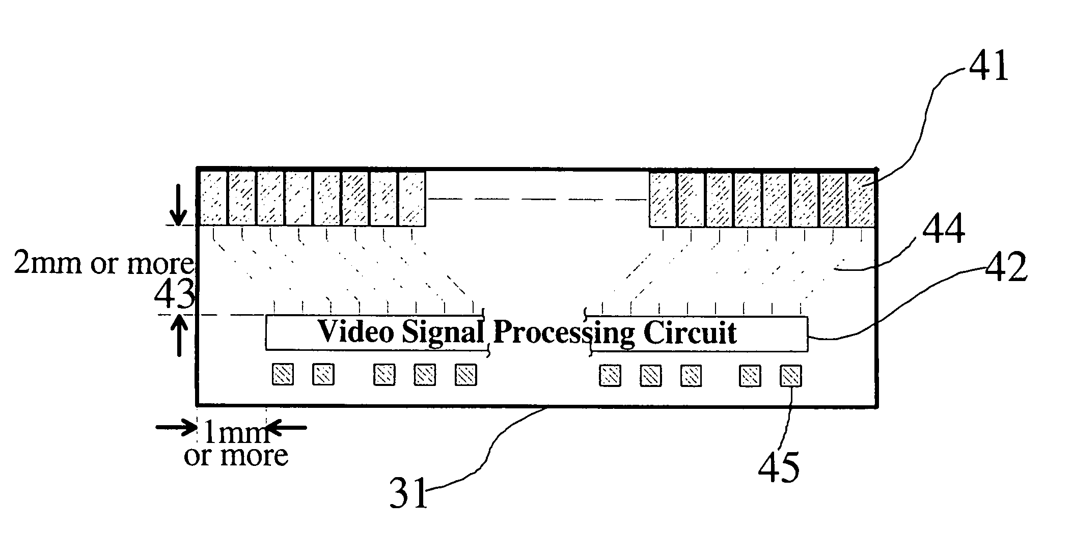
[0058]The present invention is a linear X-ray detector system 1 as illustrated in FIGS. 5, 6, and 7A-B. FIG. 7A is a sectional schematic view of the detector system 1. FIG. 7B shows a top view of the detector 1. An X-ray source 32 emits an X-ray beam 33. The X-ray beam 33 passes through a metal aperture 34, resulting in a collimated X-ray beam 35 downstream of the aperture 34. A test specimen 36 is positioned underneath the collimated X-ray beam 35. The test specimen 36 modulates the X-ray beam 35 according to the pattern and material density of the test specimen 36. The modulated X-ray pattern is then detected and an image produced by the detector unit placed under the test specimen 36.

[0059]The detector unit comprises a long detector array 3 bonded on a PCB substrate 2. (The detector array 3, formed by butting multiple chips of monolithic detector array 31 end-to-end, is described in further detail below with reference to FIG. 6.) A scintillating layer 4 is placed or deposited on ...


PUM


Abstract

A radiation damage resistant linear X-ray detector array system based on a unique buttable monolithic image sensor design and precision chip-on-board assembly technology includes at least one of the detector chips. Multiple chips of the image sensor may be butted end-to-end on a common printed circuit board to accommodate larger detection systems. A layer of scintillating material, such as Gd2O2S:Tb (GOS), CsI(Tl), or CdWO4, is placed on the image sensor to convert the impinging X-ray energies into visible light which can be detected efficiently by the image sensor array. A protective metal shield is fastened to the substrate to protect the sensitive circuits of the image sensor from X-ray radiation damage. A proper separation of sensitive circuits from the photodiode array on the sensor chip, coupled with precision registration of the sensor chips on the substrate, allows easy installation of the protective metal shield.

Description

BACKGROUND OF THE INVENTION[0001]1. Field of the Invention[0002]The present invention pertains generally to the field of solid-state X-ray imaging systems and displays, and more particularly is an X-ray system utilizing a buttable monolithic photodiode detector array. The monolithic photodiode detector array includes both the photodiode array circuits and the peripheral circuits spaced apart from the photodiode array circuits to allow precision shielding of the peripheral circuits from x-ray radiation damage.[0003]2. Description of the Prior Art[0004]As used in this disclosure, X-rays are defined as ionizing electromagnetic radiation that is damaging to semiconductor-based image sensor arrays. X-rays also include the radiation known as “extreme ultraviolet radiation” and “gamma rays”. Since few X-rays with energies exceeding 10 keV can be captured by commonly used semiconductor-based image sensor arrays (arrays using Si, Ge, etc.), the X-ray energies must be converted into a detecta...

Claims


Application Information

Patent Timeline
Patent Type & Authority Patents(United States)
IPC IPC(8): H01L27/146H01L27/00
CPCH01L27/14618H01L27/14623H01L27/14663H01L2224/48091H01L2224/49175H01L2224/05553H01L2924/00014
Inventor TSENG, HSIN-FUYANG, LIN-BOLI, SHIZU
Owner X SCAN IMAGING CORP
Features
  • R&D
  • Intellectual Property
  • Life Sciences
  • Materials
  • Tech Scout
  • Unparalleled Data Quality
  • Higher Quality Content
  • 60% Fewer Hallucinations
Learn More