Method and arrangement for producing an N-semiconductive indium sulfide thin layer

a technology of semi-conductive indium sulfide and thin film, which is applied in the direction of individual semiconductor device testing, semiconductor/solid-state device testing/measurement, instruments, etc., can solve the problems of poor film adhesion and homogeneity, inability to meet the requirements of the substrate, and inherently slow and hardly suitable process

Inactive Publication Date: 2012-03-27
HELMHOLTZ ZENT BERLIN FUER MATERIALIEN & ENERGIE GMBH
View PDF18 Cites 2 Cited by
  • Summary
  • Abstract
  • Description
  • Claims
  • Application Information

AI Technical Summary

Problems solved by technology

However, to date, CVD methods are not used for producing it because the materials to be used tend to form solid reaction products already in the gas phase, resulting in inhomogeneous films with poor coverage on the substrate.
Due to this procedure, the process is inherently very slow and hardly suitable for producing films having thicknesses of several 10 nm on an industrial scale.
Moreover, unreacted atoms of the first precursor in lower layers cannot be caused to undergo reaction later, and may therefore result in defects.
However, in prior art film production methods, special care must be taken to prevent contact of the two precursors during the process, because otherwise premature reaction (i.e., powder formation) may occur in the gas phase, which would result in poor film adhesion and homogeneity, and thus in films of inferior quality.
Photovolt: Res. Appl. 2003; 11:437-443, an ALCVD method for buffer layers of solar cells is described, in which indium acetylacetonate In(acac)3 evaporated at 125° C. and H2S gas are used at substrate temperatures of 160° C. to 260° C. However, it is generally understood by those skilled in the art that such a method is far too slow and too expensive to be used for producing solar cells on an industrial scale.
However, in this method, temperatures between 350° C. and 650° C. are required to crack the organometallic compounds which are used as precursors and which first have to be prepared from metal halides or the like, which is complicated and expensive.
U.S. Pat. No. 5,112,650 describes that in chemical vapor deposition of metal chalcogenide thin films, addition of hydrogen sulfide to the carrier gas is theoretically possible, but in practice not suitable in the case of insoluble metal sulfides, because it results in unwanted powder formation and, thus, inhomogeneous film formation.

Method used


Image

  • Method and arrangement for producing an N-semiconductive indium sulfide thin layer
  • Method and arrangement for producing an N-semiconductive indium sulfide thin layer
  • Method and arrangement for producing an N-semiconductive indium sulfide thin layer

Examples


Embodiment Construction

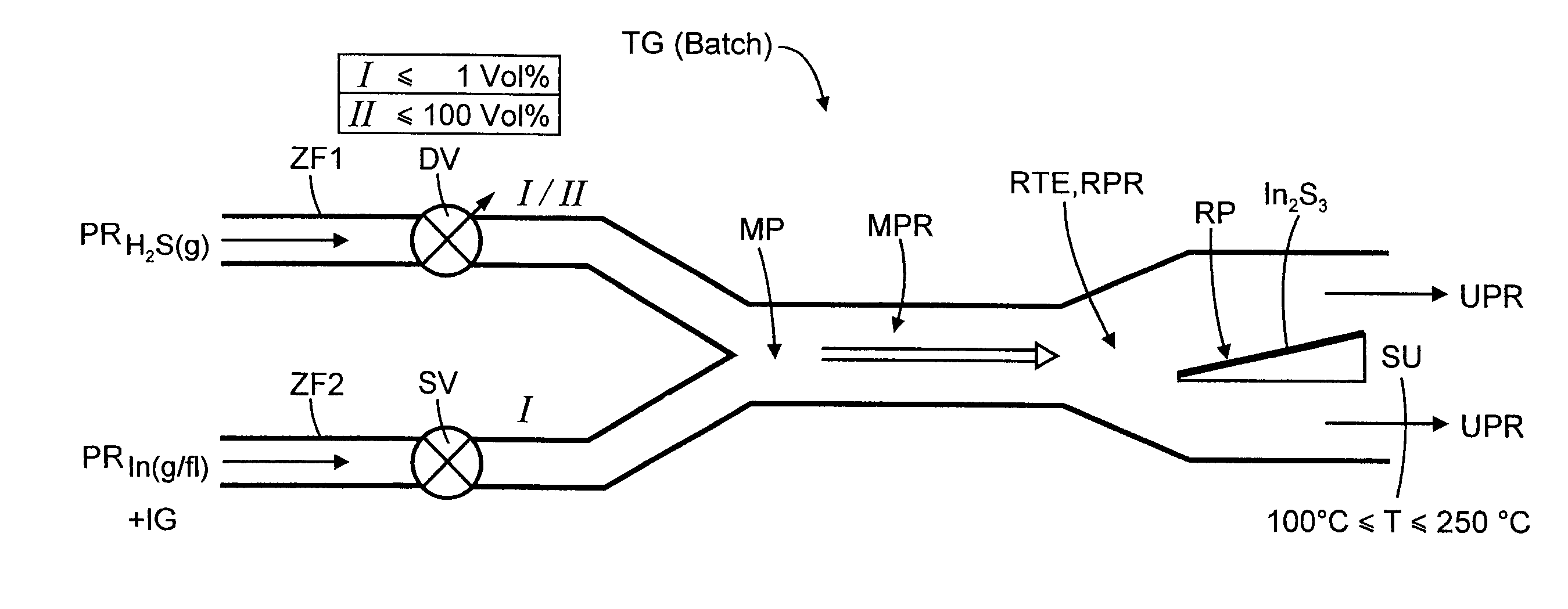
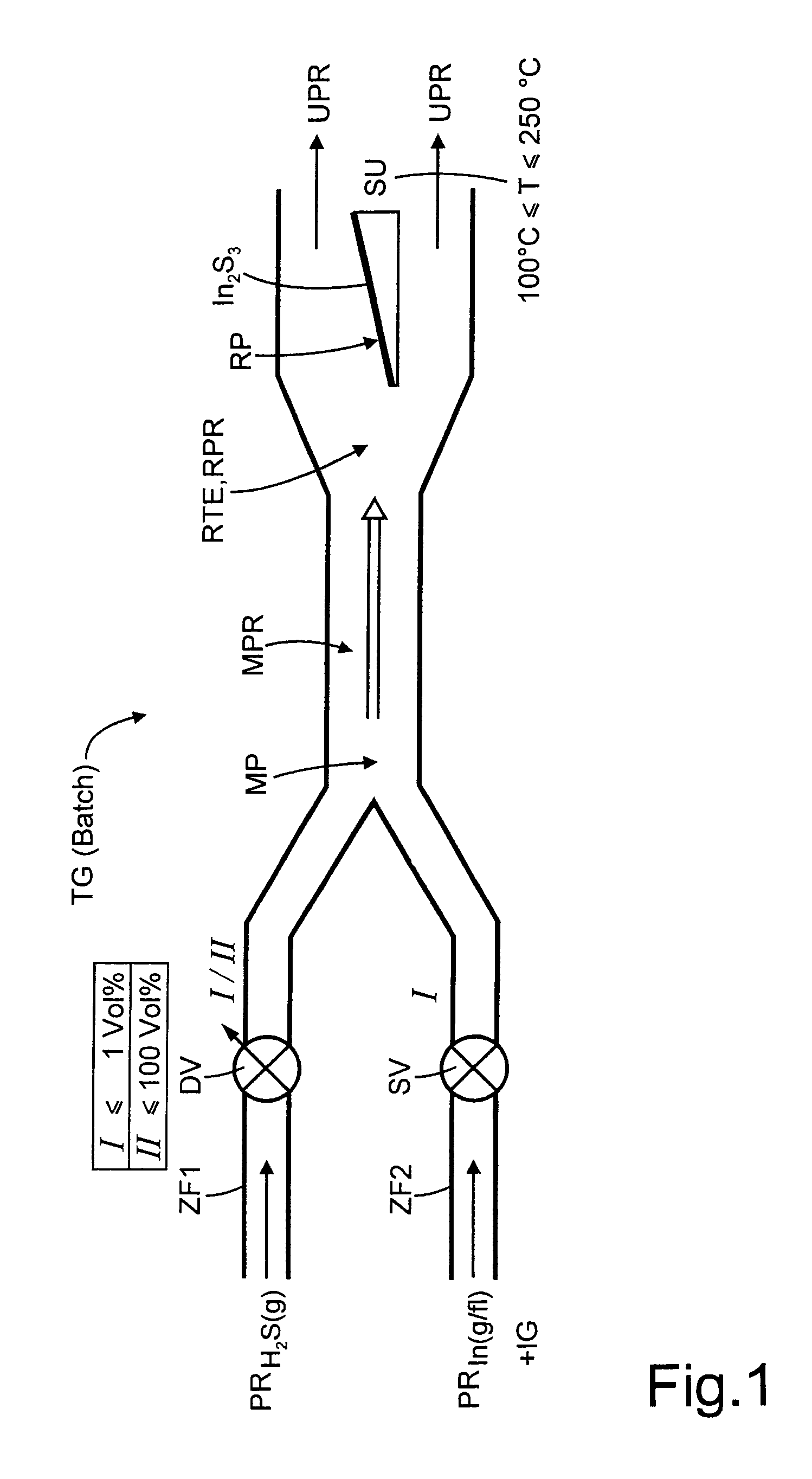
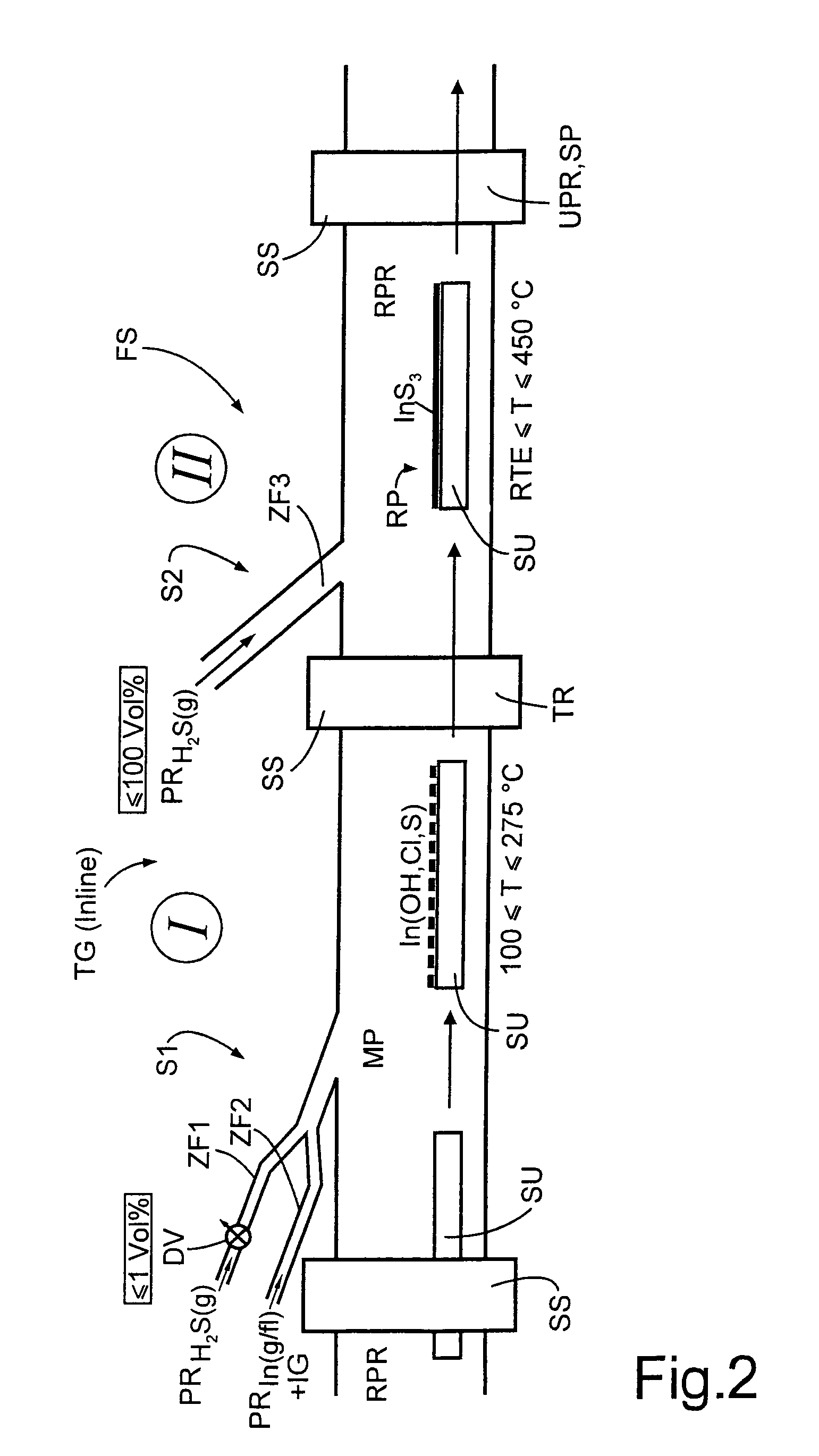
[0015]In an embodiment, an aspect of the present invention is to improve the above-described (“spray ILGAR”) method for producing indium sulfide thin films (In2S3) on a heated substrate using a sprayable, indium-containing precursor and hydrogen sulfide as a reactive gaseous precursor, and to do so in such a way that particularly homogeneous and compact indium sulfide films of constant quality can be produced, taking account of economic and ecological aspects, while at the same time further improving the material utilization and deposition rate. A system is provided to implement the improved method in a particularly simple and inexpensive manner.

[0016]In an embodiment of the method of the present invention, a spray ILGAR method is enhanced by a CVD process step, more specifically, by an atmospheric pressure chemical vapor deposition (APCVD) process step (CVD at atmospheric pressure), while maintaining its advantages mentioned in the publications cited above, a simultaneous process b...


PUM

PropertyMeasurementUnit
temperatureaaaaaaaaaa

Abstract

A method of producing, at atmospheric pressure, an n-type semiconductive indium sulfide thin film on a substrate using an indium-containing precursor, hydrogen sulfide as a reactive gaseous precursor, and an inert carrier gas stream includes cyclically repeating first and second steps so as to produce an indium sulfide thin film of a desired thickness. The first method phase includes converting the indium-containing precursor to at least one of a dissolved and a gaseous phase, heating the substrate to a temperature in a range of 100° C. to 275° C., directing the indium containing precursor onto the substrate and supplying hydrogen sulfide to the indium-containing precursor in a mixing zone in an amount so as to provide an absolute concentration of hydrogen sulfide that is greater than zero and no greater than 1% by volume. The indium concentration of the indium-containing precursor is set so as to produce a compact In(OHx,Xy,Sz)3 film, where X=halide and x+y+2z=1 with z≠0. The second step includes setting a temperature of the substrate in a range of 18° C. and 450° C. and directing hydrogen sulfide onto the substrate in an absolute concentration up to 100%.

Description

CROSS REFERENCE TO RELATED APPLICATIONS[0001]This application is a U.S. National Phase application under 35 U.S.C. §371 of International Application No. PCT / DE2009 / 000353, filed on Mar. 14, 2009, and claims benefit to German Patent Application No. DE 10 2008 017 077.1, filed on Apr. 1, 2008. The International Application was published in German on Oct. 8, 2009 as WO 2009 / 121318 A1 under PCT Article 21 (2).FIELD[0002]The present invention relates to a method for producing an n-type semiconductive indium sulfide thin film (In2S3) on a heated substrate at atmospheric pressure, using a two-source precursor including an indium-containing precursor (PRIn(g / li)), hydrogen sulfide (H2S) as a reactive gaseous precursor, and an inert carrier gas stream.BACKGROUND[0003]N-type semiconductive metal sulfide thin films are used as buffer layers between the window layer and the absorber layer in solar cells, thereby allowing a significant increase in efficiency. A “buffer layer” is understood to be...

Claims


Application Information

Patent Timeline
Patent Type & Authority Patents(United States)
IPC IPC(8): H01L21/36H01L21/20H01L21/76H01L21/469
CPCC23C16/305C23C16/45527
Inventor ALLSOP, NICHOLASFISCHER, CHRISTIAN-HERBERTGLEDHILL, SOPHIELUX-STEINER, MARTHA CHRISTINA
Owner HELMHOLTZ ZENT BERLIN FUER MATERIALIEN & ENERGIE GMBH
Why Eureka
Try Eureka