Data transfer flows for on-chip folding

a data transfer flow and chip technology, applied in the field of reprogrammable nonvolatile memory systems, can solve the problems of prone to mechanical failure, unsuitable mobile and handheld environment for conventional mass storage, and bulky disk drives

Active Publication Date: 2012-03-27
SANDISK TECH LLC
View PDF152 Cites 122 Cited by
  • Summary
  • Abstract
  • Description
  • Claims
  • Application Information

AI Technical Summary

Problems solved by technology

Conventional mass storage, based on rotating magnetic medium such as hard drives and floppy disks, is unsuitable for the mobile and handheld environment.
This is because disk drives tend to be bulky, are prone to mechanical failure and have high latency and high power requirements.
These undesirable attributes make disk-based storage impractical in most mobile and portable applications.
This method of update is inefficient, as it requires an entire erase block to be erased and rewritten, especially if the data to be updated only occupies a small portion of the erase block.
It will also result in a higher frequency of erase recycling of the memory block, which is undesirable in view of the limited endurance of this type of memory device.
Along with such large capacity operating units the challenge is to operate them efficiently.
Another problem with managing flash memory system has to do with system control and directory data.
However, with an intervening file management system between the controller and the flash memory, the data can not be accessed as directly.
Also, system control and directory data tends to be active and fragmented, which is not conducive to storing in a system with large size block erase.
This process takes time and requires controller RAM capacity, all the more so with ever increasing flash memory capacity.
Prior art systems tend to have the update data distributed over many blocks or the update data may render many existing blocks partially obsolete.
The result often is a large amount of garbage collection necessary for the partially obsolete blocks, which is inefficient and causes premature aging of the memory.
Also, there is no systematic and efficient way of dealing with sequential update as compared to non-sequential update.

Method used


Image

  • Data transfer flows for on-chip folding
  • Data transfer flows for on-chip folding
  • Data transfer flows for on-chip folding

Examples


Embodiment Construction

Memory System

[0053]FIG. 1 to FIG. 7 provide example memory systems in which the various aspects of the present invention may be implemented or illustrated.

[0054]FIG. 8 to FIG. 13 illustrate one memory and block architecture for implementing the various aspects of the present invention.

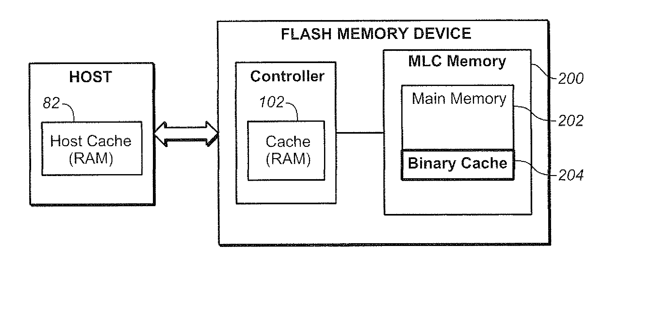
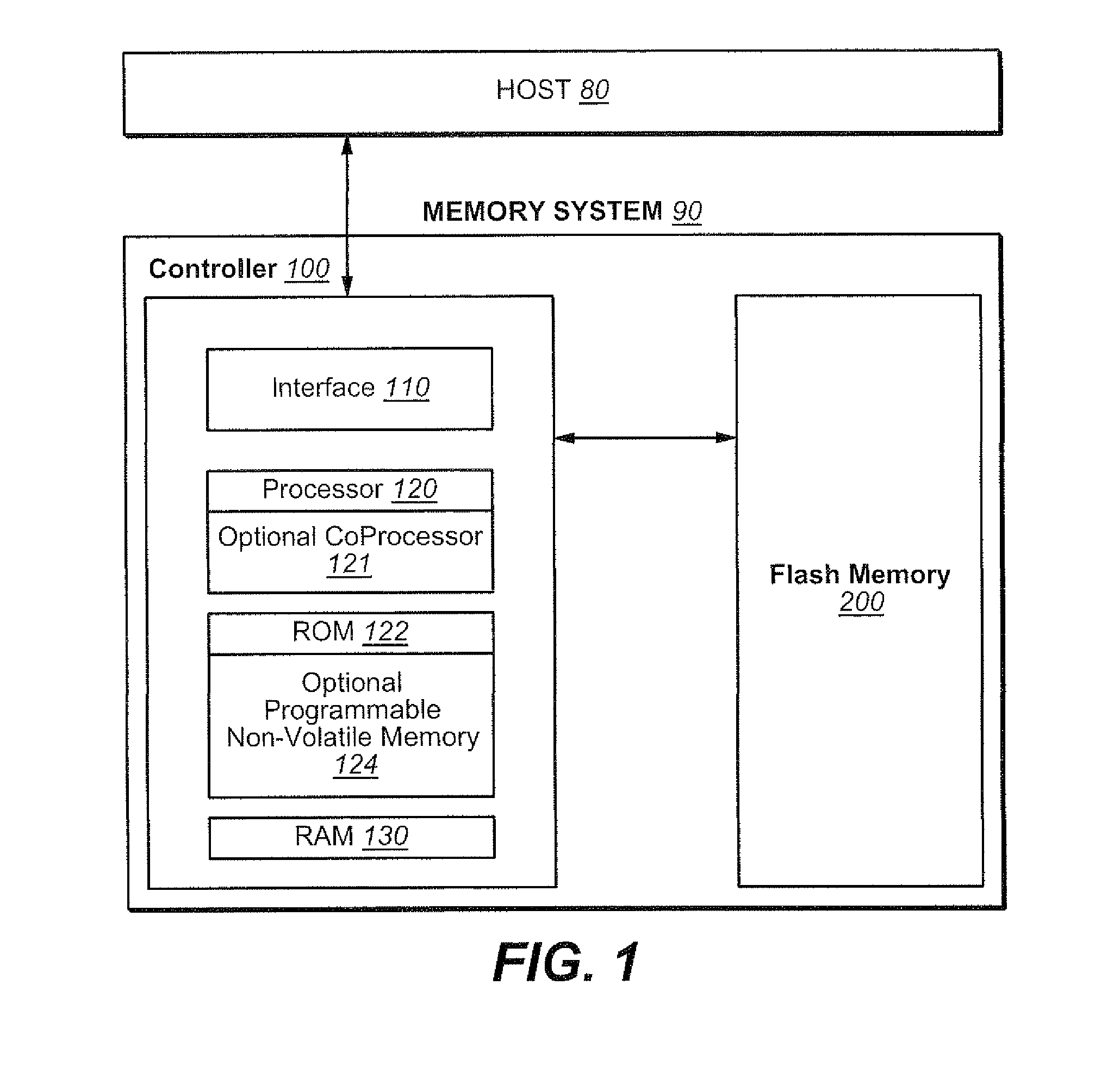
[0055]FIG. 1 illustrates schematically the main hardware components of a memory system suitable for implementing the present invention. The memory system 90 typically operates with a host 80 through a host interface. The memory system is typically in the form of a memory card or an embedded memory system. The memory system 90 includes a memory 200 whose operations are controlled by a controller 100. The memory 200 comprises of one or more array of non-volatile memory cells distributed over one or more integrated circuit chip. The controller 100 includes an interface 110, a processor 120, an optional coprocessor 121, ROM 122 (read-only-memory), RAM 130 (random access memory) and optionally programmable ...


PUM


Abstract

A memory system and methods of its operation are presented. The memory system includes a volatile buffer memory and a non-volatile memory circuit, where the non-volatile memory circuit has a first section, where data is stored in a binary format, and a second section, where data is stored in a multi-state format. When writing data to the non-volatile memory, the data is received from a host, stored in the buffer memory, transferred from the buffer memory to into read / write registers of the non-volatile memory circuit, and then written from the read / write registers to the first section of the non-volatile memory circuit using a binary write operation. Portions of the data and then subsequently folded from the first section of the non-volatile memory to the second section of the non-volatile memory, where a folding operation includes reading the portions of the data from multiple locations in the first section into the read / write registers and performing a multi-state programming operation of the portions of the data from the read / write registers into a location the second section of the non-volatile memory. The multi-state programming operations include a first phase and a second phase and one or more of the binary write operations are performed between the phases of the multi-state programming operations.

Description

CROSS-REFERENCE TO RELATED PATENT APPLICATIONS[0001]This application is related to the following United States patent applications: one entitled “Non-Volatile Memory with Multi-Gear Control Using On-Chip Folding of Data” by Huang et al. and having U.S. Published Application No. 2011 / 0153913A1; and one entitled “Maintaining Updates of Multi-Level Non-Volatile Memory in Binary Non-volatile Memory” by Gorobets et al. and having U.S. Published Application No. 1022 / 0153912A1, both of which are being filed concurrently herewith.BACKGROUND[0002]This application relates to the operation of re-programmable non-volatile memory systems such as semiconductor flash memory, and, more specifically, to the management of the interface between a host device and the memory.[0003]Solid-state memory capable of nonvolatile storage of charge, particularly in the form of EEPROM and flash EEPROM packaged as a small form factor card, has recently become the storage of choice in a variety of mobile and handhe...

Claims


Application Information

Patent Timeline
Patent Type & Authority Patents(United States)
IPC IPC(8): G11C11/34
CPCG06F12/0246G11C7/1042G11C11/5628G11C16/10G06F2212/7203G11C2211/5641G11C2211/5643G11C16/34
Inventor HUANG, JIANMINAVILA, CHRISGAVENS, LEE M.HUTCHINSON, NEIL DAVIDGOROBETS, SERGEY ANATOLIEVICH
Owner SANDISK TECH LLC
Why Eureka
Try Eureka