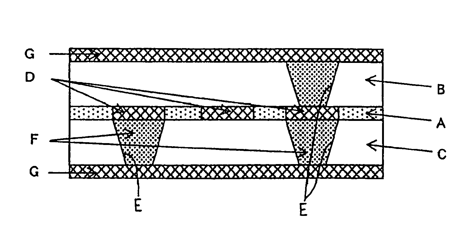
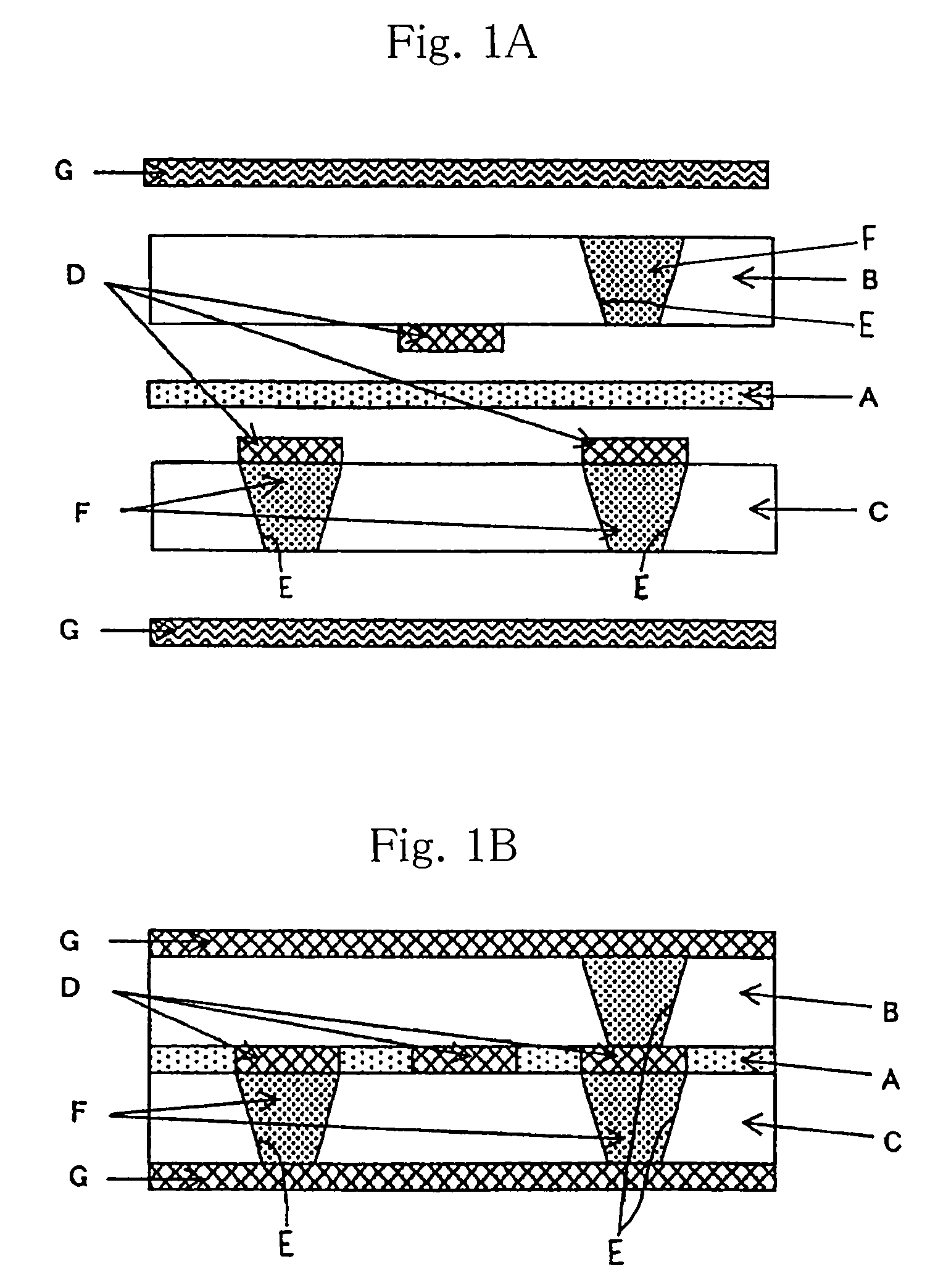
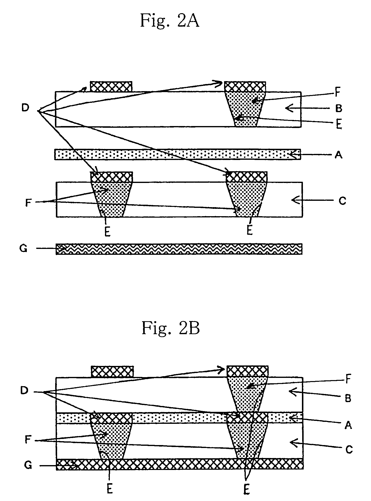
Multi-layer circuit board and method of making the same

a multi-layer circuit board and circuit board technology, applied in the direction of dielectric characteristics, electric connection formation of printed elements, electric apparatus casings/cabinets/drawers, etc., can solve the problem that the known multi-layer circuit board cannot meet the recent demand for neither can electronic parts be formed on front and rear surface regions, etc. problems, to achieve the effect of high-density surface mounting of electronic parts, simplified manufacturing process, and low melting poin

Inactive Publication Date: 2012-04-10
KURARAY CO LTD
View PDF15 Cites 2 Cited by
  • Summary
  • Abstract
  • Description
  • Claims
  • Application Information

AI Technical Summary

Benefits of technology

This approach enables high-density surface mounting of electronic parts with simplified manufacturing, reliable electric connections, and improved heat resistance, while minimizing undesirable pattern displacement and air gaps, resulting in a multi-layer circuit board with excellent electrical and thermal properties.

Problems solved by technology

It has, however, been found that the multi-layer circuit board that requires formation of holes extending through the printed wiring board and bonding layers has a problem in that neither formation of wiring nor mounting of electronic parts can be effected onto front and rear surface regions of the circuit board where holes for interlayer connection are formed.
Accordingly, not only is this known multi-layer circuit board incapable of meeting with the recent demand for a high-density surface mounting of electronic parts, but the method of making the known multi-layer circuit board includes a series of manufacturing steps, some of which appear to be redundant enough to require a complicated process control.

Method used


Image

  • Multi-layer circuit board and method of making the same
  • Multi-layer circuit board and method of making the same
  • Multi-layer circuit board and method of making the same

Examples


referential example 1

[0097]A thermoplastic liquid crystal polymer composed of a copolymer of p-hydroxybenzoic acid and 6-hydroxy-2-naphthoic acid and having a melting point of 283° C. was melt-extruded and then drawn by means of the inflation technique, wherein the draw ratio was 2.0 and the blow ratio was 6.0, to give a thermoplastic liquid crystal polymer film F1 of 20 μm in thickness and having a segment orientation ratio (SOR) of 1.03, a melting point of 283° C. and a thermal deformation temperature of 260° C.

referential example 2

[0098]A thermoplastic liquid crystal polymer composed of a copolymer of p-hydroxybenzoic acid and 6-hydroxy-2-naphthoic acid and having a melting point of 325° C. was melt-extruded and then drawn by means of the inflation technique, wherein the draw ratio was 2.0 and the blow ratio was 6.0, to give a thermoplastic liquid crystal polymer film F2 of 50 μm in thickness and having a segment orientation ratio (SOR) of 1.03, a melting point of 325° C. and a thermal deformation temperature of 305° C.

example 1

[0099]The multi-layer circuit board was obtained by the following procedures 1 to 4, which are shown respectively as FIGS. 10A to 10D.

Procedure 1:

[0100]A micro-via of a designed diameter of 100 μm was formed in the thermoplastic liquid crystal polymer film F2, obtained by the Referential Example 2, at a predetermined portion by means of a carbon dioxide laser. Thereafter, the micro-via was filled with an electroconductive paste which was subsequently cured by a preliminary heating (FIG. 10A).

Procedure 2:

[0101]An electrolytic copper foil of 18 μm in thickness was applied on each of the opposite surfaces of the thermoplastic liquid crystal polymer film F2 having the micro-via obtained by the Procedure 1. Then the stack (copper foil / thermoplastic liquid crystal polymer film / copper foil) was thermo compressed together at a temperature of 335° C. under a pressure of 3 MPa by a vacuum heat-press, to give the double-sided copper clad laminate in which the electroconductive paste filled in ...


PUM

PropertyMeasurementUnit
thicknessaaaaaaaaaa
melting pointaaaaaaaaaa
temperatureaaaaaaaaaa

Abstract

A method of making a multi-layer circuit board that has a first film and at least two more films, second and third films, each being made of a thermoplastic polymer capable of forming an optically anisotropic melt phase, the first film having a low melting point, the second and third films having respective melting points higher than the melting point of the first film and at least one of the second and the third films having a circuit pattern thereon, and the first to third films are thermo compressed together with the first film interposed between the second and third films. This method entails causing at least one of the circuit patterns on one of the second and third films to contact an opposing surface of the other of the second and third films through the first film during the thermo compression bonding of the first to third films.

Description

RELATED APPLICATIONS[0001]This application is a divisional of U.S. Ser. No. 10 / 639,648, filed on Aug. 13, 2003, which is based on Japanese Patent Application No. 2002-247974, filed on Aug. 28, 2002, the entire contents of which are hereby incorporated by reference.BACKGROUND OF THE INVENTION[0002]1. Field of the Invention[0003]The present invention relates to a multi-layer circuit board utilizing, as an insulating layer, a film made of a thermoplastic polymer capable of forming an optically anisotropic melt phase and also relates to a method of making such multi-layer circuit board.[0004]In the description of the present invention, the thermoplastic polymer capable of forming an optically anisotropic melt phase will be referred to as a “thermoplastic liquid crystal polymer” unless otherwise specified and, also, the film utilizing such thermoplastic liquid crystal polymer will be referred to as a “thermoplastic liquid crystal polymer film” unless otherwise specified.[0005]2. Descript...

Claims


Application Information

Patent Timeline
Patent Type & AuthorityPatents(United States)
IPC IPC(8): B32B37/04H05K3/38H05K3/40H05K3/46
CPCH05K3/4617H05K3/4626H05K3/4655H05K3/386H05K3/4069H05K3/4652Y10T428/24917H05K2201/0129H05K2201/0141H05K2201/0195H05K2201/09881H05K2203/1189H05K3/46
InventorTSUGARU, TOSHINORISUNAMOTO, TATSUYAYOSHIKAWA, TADAO
OwnerKURARAY CO LTD