
Complementary metal oxide semiconductor (CMOS) image sensor with extended pixel dynamic range incorporating transfer gate with potential well

a metal oxide semiconductor and image sensor technology, applied in the field of solid-state image sensors, can solve the problems of low dynamic range (dr) and low signal to noise ratio (snr), low sensitivity and increased noise, and large vdd potential level, and achieve high performan

Active Publication Date: 2012-04-17
INTELLECTUAL VENTURES II
View PDF10 Cites 8 Cited by
  • Summary
  • Abstract
  • Description
  • Claims
  • Application Information

AI Technical Summary

Benefits of technology

[0009]Embodiments of the present invention are directed toward providing a practical pixel design that can be used in a small pixel and a CMOS image sensor array with a high performance.

Problems solved by technology

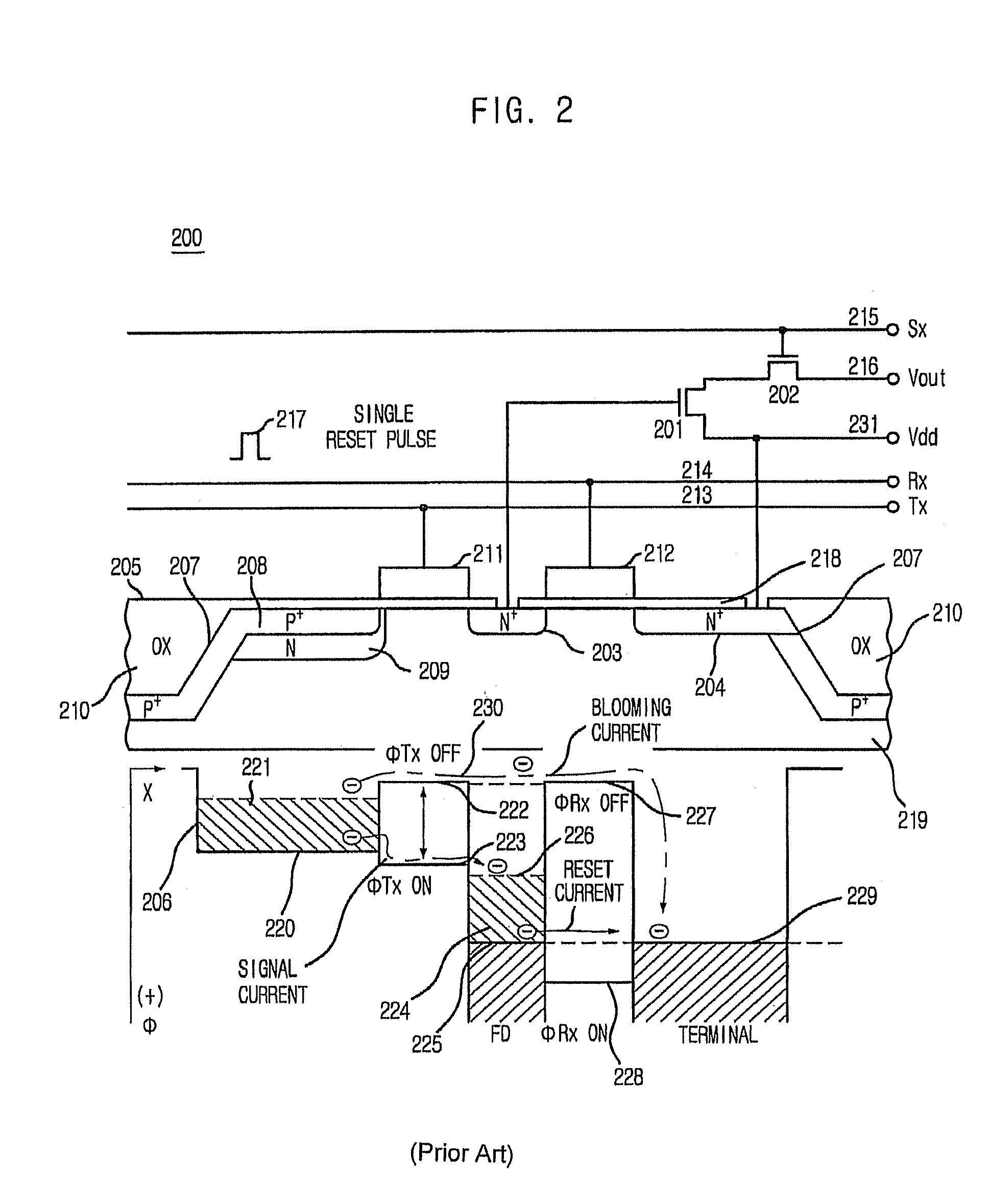
When too much signal accumulates in the photodiode 205, not all of the signal can be transferred into the FD node 203, which results in the lower sensitivity and increased noise.
However, the low pinning voltage level results in a low photodiode charge storage capacity, thereby causing a low dynamic range (DR) and a low signal to noise ratio (SNR).
To have a large Vdd potential level is a disadvantage, since the large Vdd potential level increases the sensor power consumption.

Method used


Image

  • Complementary metal oxide semiconductor (CMOS) image sensor with extended pixel dynamic range incorporating transfer gate with potential well
  • Complementary metal oxide semiconductor (CMOS) image sensor with extended pixel dynamic range incorporating transfer gate with potential well
  • Complementary metal oxide semiconductor (CMOS) image sensor with extended pixel dynamic range incorporating transfer gate with potential well

Examples


Embodiment Construction

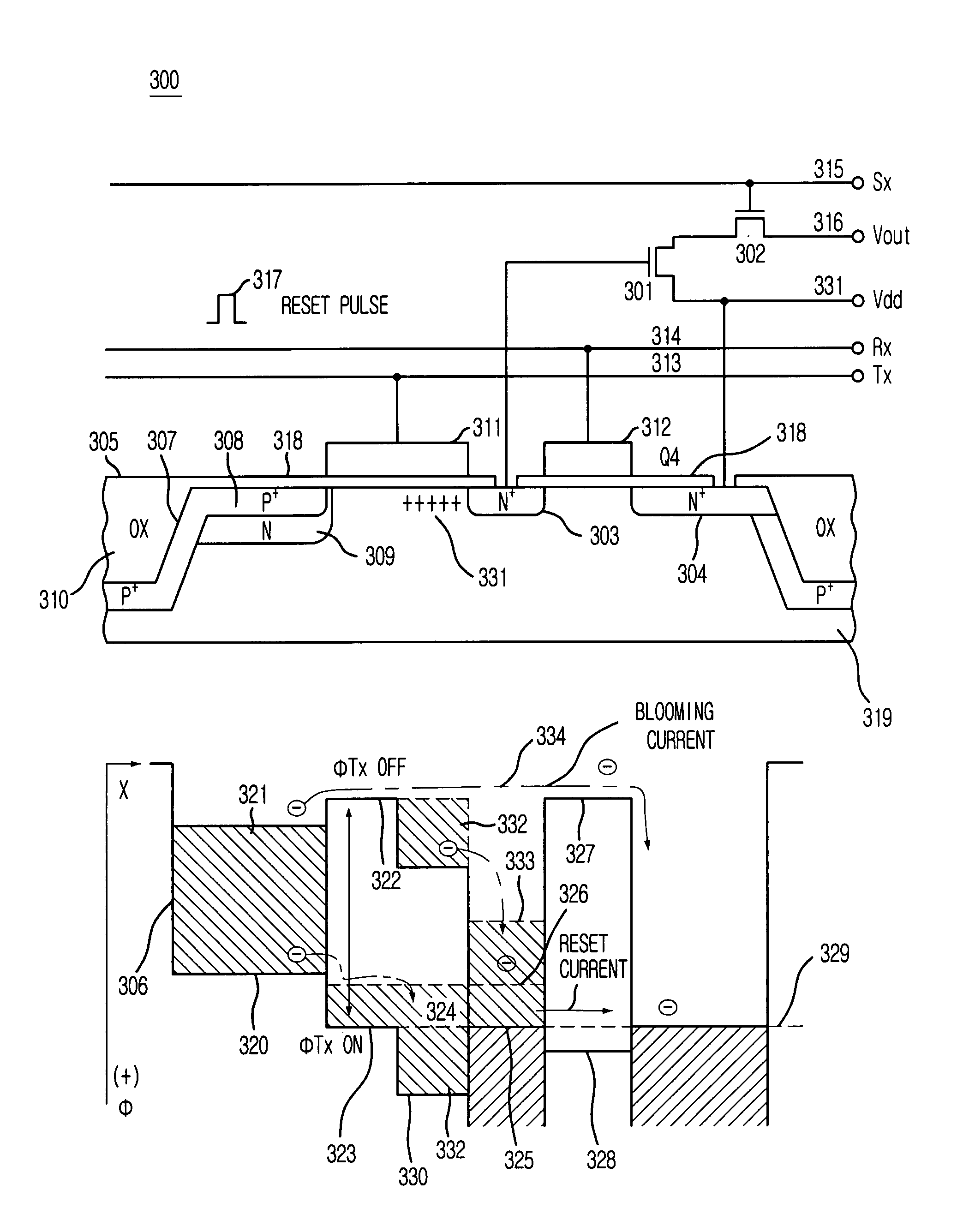
[0017]According to embodiments of the present invention, a potential well that is formed under a gate of a charge transfer transistor and interfaces with a floating diffusion (FD) node which detects a charge is used. The use of the potential well allows increasing a pinning voltage level of a photodiode above a minimum excursion of the FD node. As a result, it is possible to build a CMOS sensor array with a high charge storage capacity, a high dynamic range (DR), a large signal to noise ratio (SNR), and a very small sized pixel.

[0018]More particularly, the potential well is formed under the gate of the charge transfer transistor. Thus, a floating diffusion voltage swing is not limited by a pinning voltage level of a new gate structure of the charge transfer transistor, and as a result, a floating diffusion voltage can swing lower. The potential well under the gate of the charge transfer transistor stores an excess charge, prevents the excess charge from flowing back to the photodiod...


PUM


Abstract

A charge transfer transistor includes: a first diffusion region and a second diffusion region; a gate for controlling a charge transfer from the first diffusion region to the second diffusion region by a control signal; and a potential well incorporated under the gate, wherein the first diffusion region is a pinned photodiode. A pixel of an image sensor includes: a photodiode for generating and collecting a photo generated charge; a floating diffusion region for serving as a photo generated charge sensing node; a transfer gate for controlling a charge transfer from the photodiode to the floating diffusion region by a control signal; and a potential well incorporated under the transfer gate.

Description

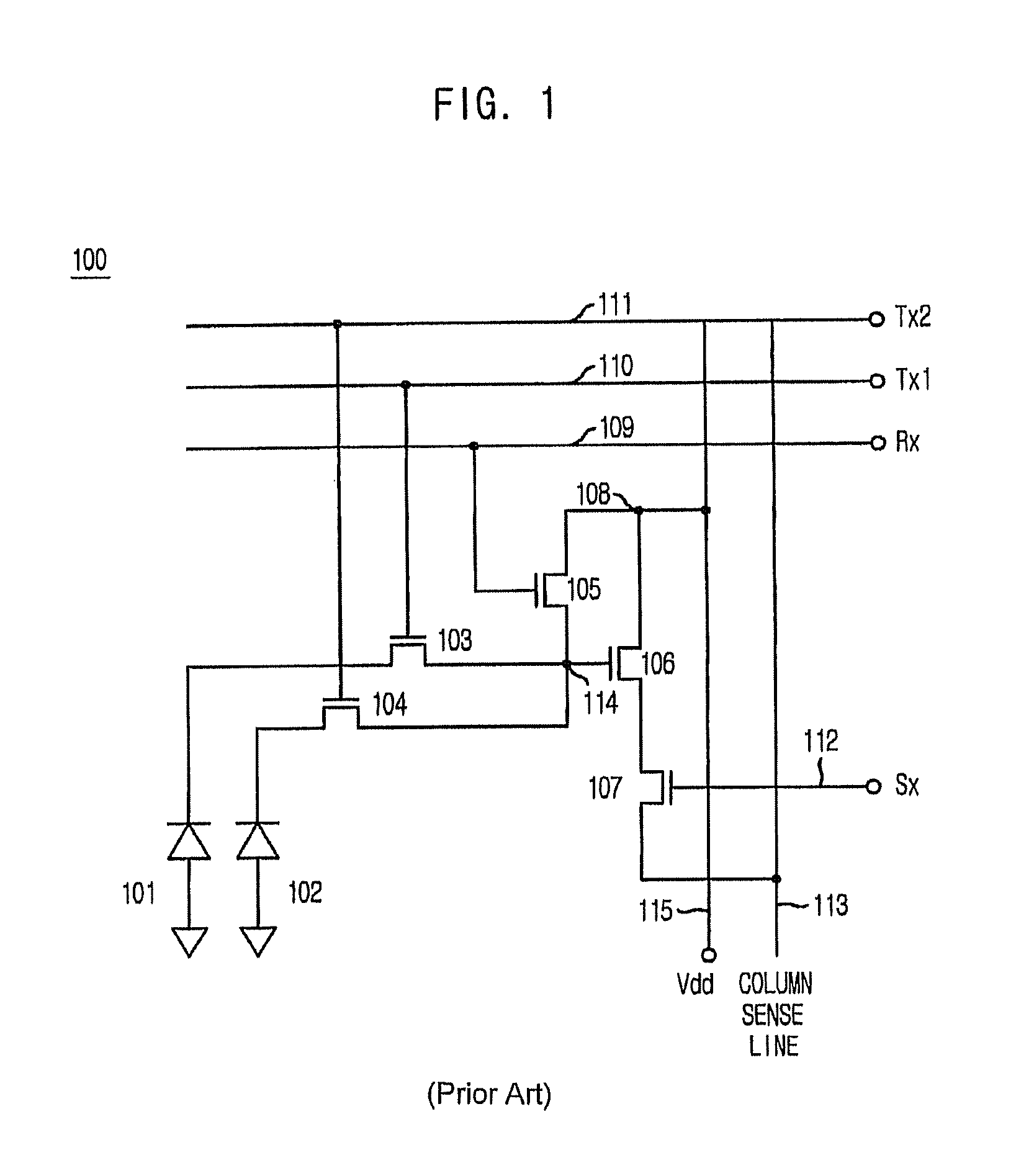
CROSS-REFERENCE TO RELATED APPLICATIONS[0001]The present invention claims priority of Korean patent application number 10-2006-0040713, filed on May 4, 2006 which is incorporated by reference in its entirety.BACKGROUND OF THE INVENTION[0002]The present invention relates to a solid-state image sensor having an improved performance with a higher charge well capacity which results in a higher dynamic range (DR) and a better signal to noise ratio (SNR), and more particularly to a complementary metal oxide semiconductor (CMOS) image sensor.[0003]A typical pixel of the CMOS image sensor includes a photodiode, more precisely a pinned photodiode, and four transistors. The photodiode collects a photo-generated charge that is later transferred at a suitable moment by a charge transfer transistor onto a floating diffusion (FD) node which detects the charge. Prior to the charge transfer, however, the FD node must be first reset by a reset transistor to a suitable reference voltage, which is usu...

Claims


Application Information

Patent Timeline
Patent Type & Authority Patents(United States)
IPC IPC(8): H01L31/102H01L27/146H04N25/00
CPCH01L27/14609H01L27/1463H04N3/155H04N5/3559H04N25/59H04N25/778H01L27/146
Inventor HYNECEK, JAROSLAV
Owner INTELLECTUAL VENTURES II
Learn More