
Display device including driver circuit and monitor circuit

a display device and driver circuit technology, applied in static indicating devices, non-linear optics, instruments, etc., can solve the problems of serious shift of threshold voltage due to charge trapping, charge is trapped, etc., to achieve accurate grasping increase the reliability of the display device, and increase the accuracy of the amount of change of the threshold voltage of the output circui

Active Publication Date: 2012-04-24
SEMICON ENERGY LAB CO LTD
View PDF16 Cites 14 Cited by
  • Summary
  • Abstract
  • Description
  • Claims
  • Application Information

AI Technical Summary

Benefits of technology

The present invention provides a display device that can compensate for a shift in the threshold voltage of a thin film transistor (TFT) in an output circuit caused by trapping of charge in the gate insulating film. By applying a reverse bias voltage to the gate of the TFT, the threshold voltage can be reversed and compensated for. This ensures high reliability of the driver circuit even when the threshold voltage shifts. The display device includes a power supply control circuit, a monitor transistor, and a threshold control circuit. The monitor transistor monitors the change in the threshold voltage of the TFT and the threshold control circuit controls the power supply control circuit to apply the reverse bias voltage at the right time to compensate for the threshold voltage shift.

Problems solved by technology

However, a threshold voltage of a thin film transistor using a gate insulating film containing nitrogen largely shifts as an absolute value of a voltage applied to a gate is large and as on-state time (driving time) is long.
This is because charge is trapped in the gate insulating film when a voltage is applied to the gate.
In particular, in the case where a thin film transistor using an amorphous semiconductor is used, there are many cases in which an insulating film containing nitrogen is used for a gate insulating film; therefore, a shift of a threshold voltage due to trapping of charge is a serious problem.

Method used


Image

  • Display device including driver circuit and monitor circuit
  • Display device including driver circuit and monitor circuit
  • Display device including driver circuit and monitor circuit

Examples


embodiment mode 1

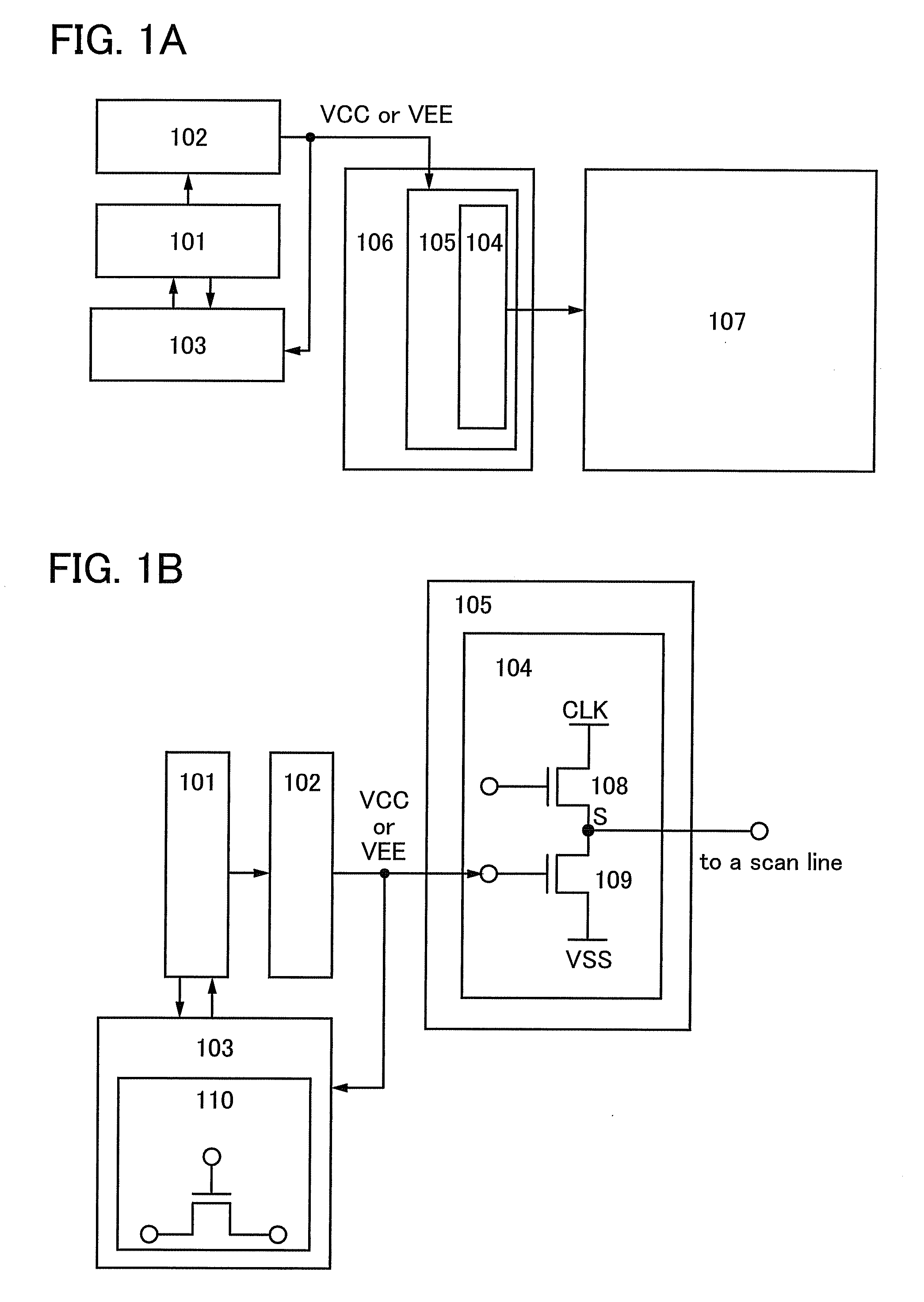
[0048]A structure of a display device of the present invention will be described with reference to FIGS. 1A and 1B. FIG. 1A is a block diagram of the display device of the present invention. The display device of the present invention includes a threshold control circuit 101, a power supply control circuit 102, a monitor circuit 103, and an output circuit 104. The display device of the present invention shown in FIG. 1A further includes a shift register 105 having the output circuit 104, a scan line driver circuit 106 having the shift register 105, and a pixel portion 107. In addition to the above structure, the display device of the present invention may also include a signal line driver circuit.

[0049]The pixel portion 107 is provided with a plurality of pixels, and the pixels are selected per line by the scan line driver circuit 106. A signal line driver circuit controls the input of a video signal to the pixels of the line selected by the scan line driver circuit 106.

[0050]The sh...

embodiment mode 2

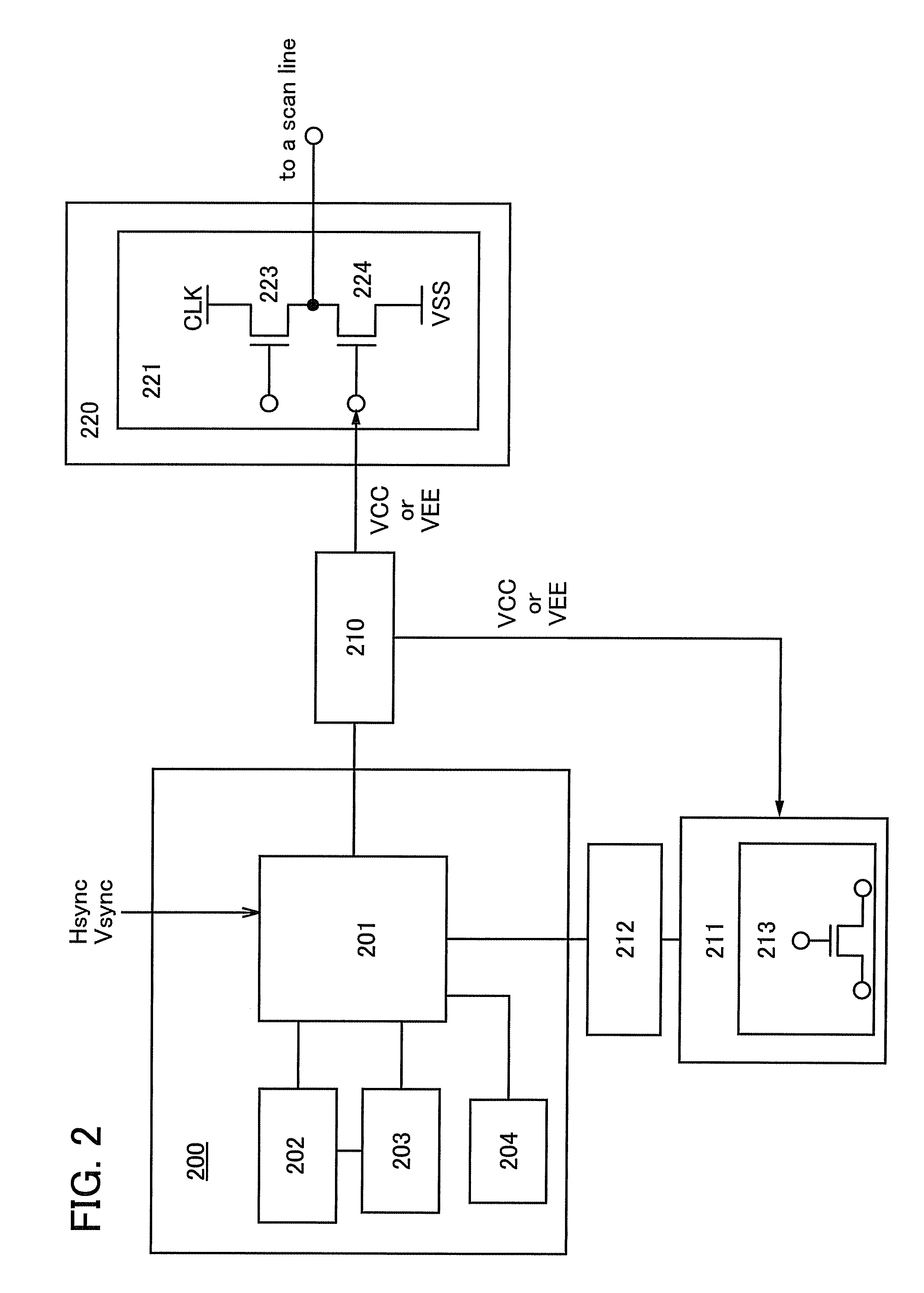
[0069]In this embodiment mode, an example of a specific structure of a threshold control circuit included in the display device of the present invention will be described. A threshold control circuit 200 shown in FIG. 2 includes a controller 201, an arithmetic circuit 202, a measurement circuit 203, and a memory 204. In FIG. 2, a power supply control circuit 210, a monitor circuit 211, and an AD converter circuit 212 are also shown.

[0070]An output circuit 221 included in a shift register 220 includes a transistor 223 and a transistor 224 which are connected in series. In a period when an image is displayed on a pixel portion, a voltage of a clock signal CLK is applied to either one of a source and a drain of the transistor 223, and the other thereof is connected to a scan line. A voltage VSS is applied to a source of the transistor 224, and a drain of the transistor 224 is connected to the scan line. Therefore, the clock signal CLK is sampled by the transistor 223, and the supply of...

embodiment mode 3

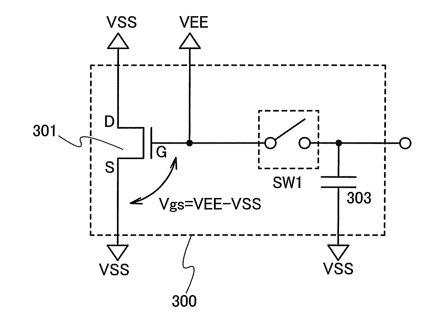
[0082]In this embodiment mode, a specific structure of a monitor circuit will be described. As shown in FIG. 4, a monitor circuit 300 of the present invention includes a monitor transistor 301. In addition, the monitor circuit 300 of the present invention may include a capacitor 303 and a switching element SW1 as shown in FIG. 4.

[0083]A drain (D) side of the monitor transistor 301 is provided with a switching element SW2 which can control application of a voltage VIN1. A gate (G) side of the monitor transistor 301 is provided with a switching element SW3 which can control application of a voltage VIN2. Further, a switching element SW4 which controls connection of a gate and a drain of the monitor transistor 301 is provided. Note that application of a voltage to the drain and the gate of the monitor transistor 301 can be controlled from the outside of the monitor circuit 300 as well as from the inside thereof. Accordingly, the switching element SW2, the switching element SW3, and the...


PUM


Abstract

To provide a display device which can ensure high reliability of a driver circuit even when a threshold voltage of a TFT shifts. The display device includes a power supply control circuit which can apply a forward bias voltage or a reverse bias voltage to a gate of a transistor included in an output circuit, a monitor transistor which is formed to monitor the amount of change of a threshold voltage of the transistor included in the output circuit, and a threshold control circuit which controls the power supply control circuit so as to apply the reverse bias voltage to the gate of the transistor in order to compensate the threshold voltage of the transistor included in the output circuit.

Description

BACKGROUND OF THE INVENTION[0001]1. Field of the Invention[0002]The present invention relates to a display device using a thin film transistor.[0003]2. Description of the Related Art[0004]Display devices formed using inexpensive glass substrates tend to be prevented from being downsized due to increase in the ratio of a region (frame region) at the periphery of a pixel portion used for mounting to a substrate, as the resolution increases. Accordingly, it is thought that there is a limitation on a method in which a driver circuit formed using a single crystal semiconductor substrate is mounted on a glass substrate, and a technique by which a driver circuit is formed over the same glass substrate as a pixel portion, a so-called system-on-panel is regarded as important. Realization of system-on-panel reduces the number of pins which are formed to connect a driver circuit and a pixel portion, and enables to avoid problems such as decrease in yield due to poor connection between the driv...

Claims


Application Information

Patent Timeline
Patent Type & Authority Patents(United States)
IPC IPC(8): G09G3/36G09G3/30
CPCG09G3/3677G09G2300/0417G09G2310/0267G09G2320/043G09G2320/048G02F1/133G09G3/20G09G3/36
Inventor MIYAKE, HIROYUKIUMEZAKI, ATSUSHI
Owner SEMICON ENERGY LAB CO LTD
Learn More