Zinc oxide film method and structure for CIGS cell

a thin film, photovoltaic cell technology, applied in the direction of coatings, semiconductor devices, chemical vapor deposition coatings, etc., can solve the problems of reducing the conversion efficiency of zinc oxid

Inactive Publication Date: 2012-05-01
CM MFG
View PDF221 Cites 32 Cited by
  • Summary
  • Abstract
  • Description
  • Claims
  • Application Information

AI Technical Summary

Benefits of technology

[0009]According to embodiments of the present invention, a method and a structure for forming a photovoltaic cell is provided. More particularly, the present invention provides a method and structure for forming thin film tandem photovoltaic cell. Merely by way of example, embodiments according to the present invention have been implemented using thin film semiconductor material. But it would be recognized that embodiments according to the present invention can have a much broader range of applicability.

Problems solved by technology

Unfortunately, the supply of petrochemical fuel is limited and essentially fixed based upon the amount available on the planet Earth.
Additionally, as more people use petroleum products in growing amounts, it is rapidly becoming a scarce resource, which will eventually become depleted over time.
Although solar energy is environmentally clean and has been successful to a point, many limitations remain to be resolved before it becomes widely used throughout the world.
However, crystalline materials are often costly and difficult to make on a large scale.
Additionally, devices made from such crystalline materials often have low energy conversion efficiencies.
Similar limitations exist with the use of thin film technology in making solar cells.
That is, efficiencies are often poor.
Additionally, film reliability is often poor and cannot be used for extensive periods of time in conventional environmental applications.
Often, thin films are difficult to mechanically integrate with each other.

Method used


Image

  • Zinc oxide film method and structure for CIGS cell
  • Zinc oxide film method and structure for CIGS cell
  • Zinc oxide film method and structure for CIGS cell

Examples


Embodiment Construction

[0015]According to embodiments of the present invention, a method and a structure for forming a photovoltaic cell are provided. More particularly, embodiments according to the present invention provide a method and structure for forming a thin film photovoltaic cell. Merely by way of example, embodiments according to the present invention have been implemented using thin film semiconductor material. But it would be recognized that embodiments according to the present invention can have a much broader range of applicability.

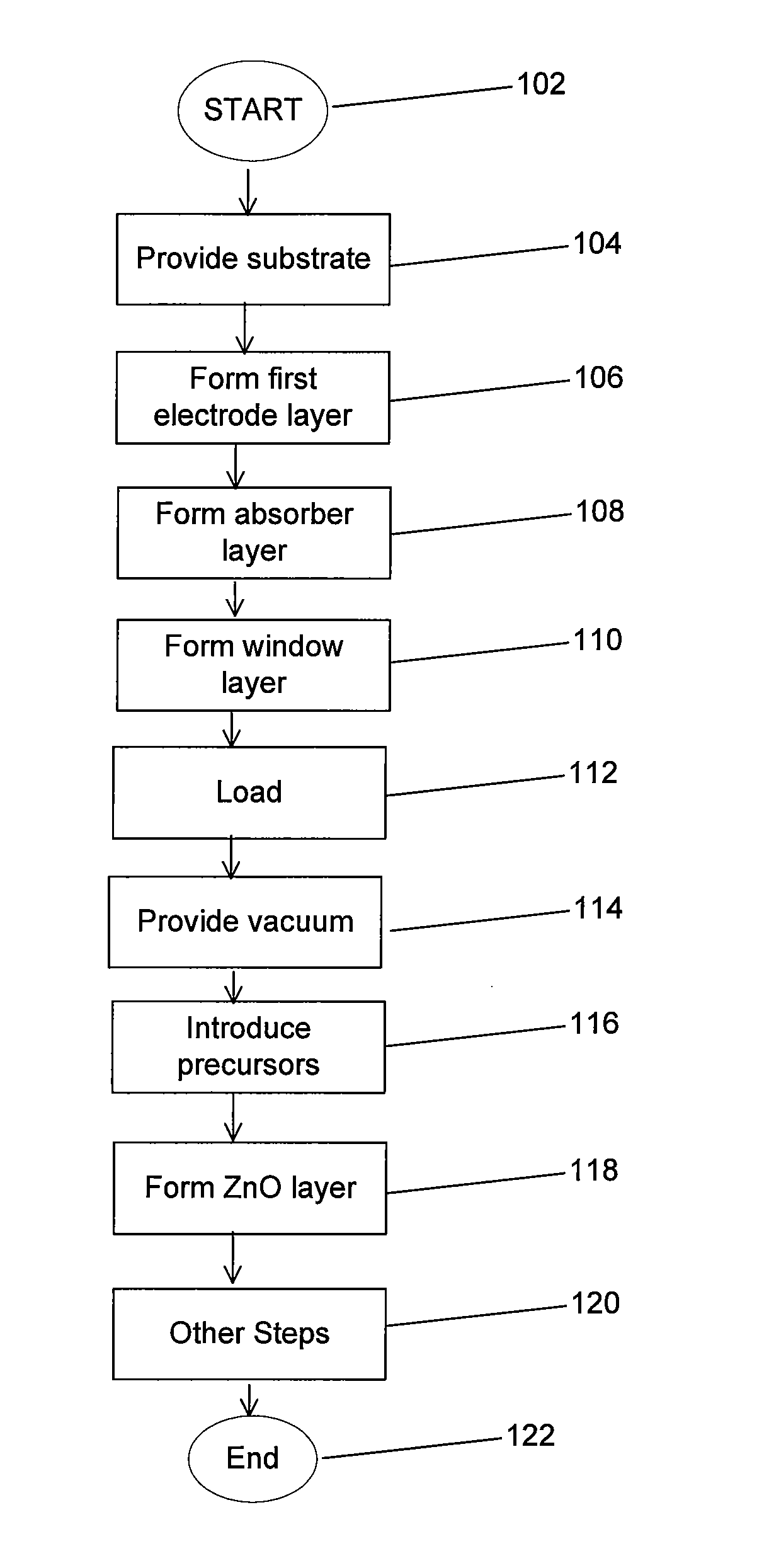
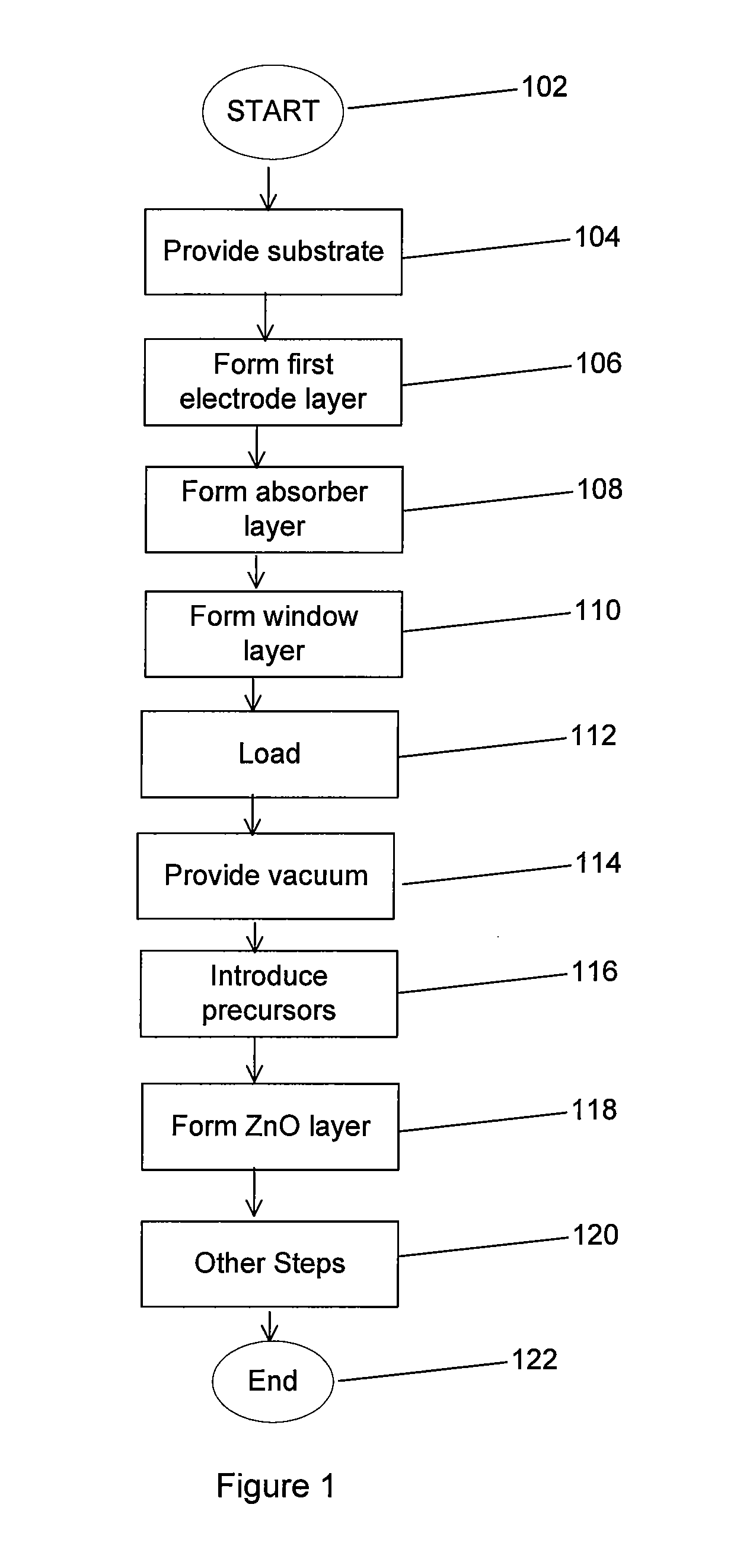
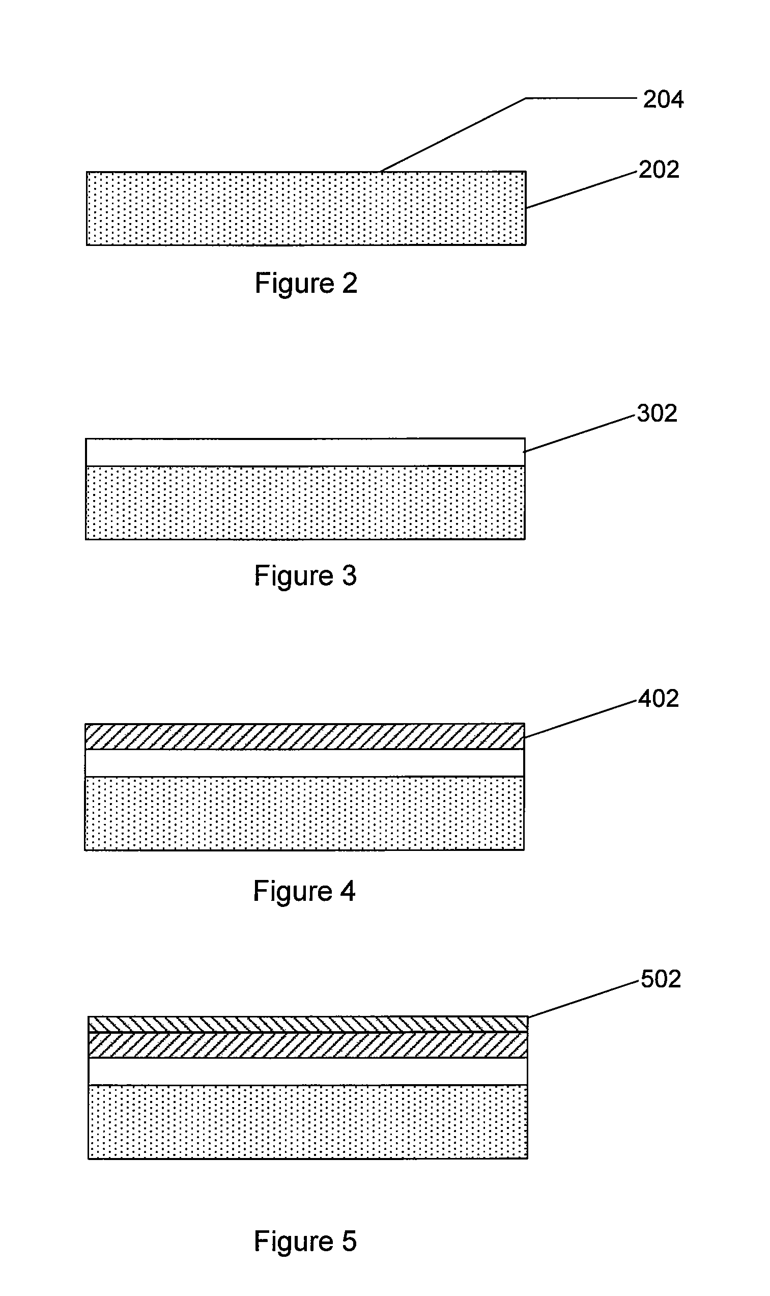
[0016]FIG. 1 is a simplified process flow diagram illustrating a method of forming a photovoltaic cell according to an embodiment of the present invention. As shown, the method begins with a Start step (Step 102). A transparent substrate is provided. The transparent substrate can use a glass substrate such as soda lime glass in a specific embodiment. Other transparent substrate materials may also be used. These other transparent substrate material can include fuse...


PUM

PropertyMeasurementUnit
temperatureaaaaaaaaaa
grain sizeaaaaaaaaaa

Abstract

A method for fabricating a thin film photovoltaic device. The method includes providing a substrate comprising an absorber layer and an overlying window layer. The substrate is loaded into a chamber and subjected to a vacuum environment. The vacuum environment is at a pressure ranging from 0.1 Torr to about 0.02 Torr. In a specific embodiment, a mixture of reactant species derived from diethylzinc species, water species and a carrier gas is introduced into the chamber. The method further introduces a diborane species using a selected flow rate into the mixture of reactant species. A zinc oxide film is formed overlying the window layer to define a transparent conductive oxide using the selected flow rate to provide a resistivity of about 2.5 milliohm-cm and less and an average grain size of about 3000 to 5000 Angstroms.

Description

CROSS-REFERENCES TO RELATED APPLICATIONS[0001]This application claims priority to U.S. Provisional Application No. 61 / 106,158 filed Oct. 17, 2008, commonly assigned, and incorporated by reference in its entirety herein for all purpose.STATEMENT AS TO RIGHTS TO INVENTIONS MADE UNDER FEDERALLY SPONSORED RESEARCH AND DEVELOPMENT[0002]Not ApplicableREFERENCE TO A “SEQUENCE LISTING,” A TABLE, OR A COMPUTER PROGRAM LISTING APPENDIX SUBMITTED ON A COMPACT DISK[0003]Not ApplicableBACKGROUND OF THE INVENTION[0004]The present invention relates generally to photovoltaic materials and manufacturing method. More particularly, the present invention provides a method and structure for a thin film photovoltaic cell. Merely by way of example, the present method and structure provide for a thin film photovoltaic cell using an absorber material comprising a copper indium disulfide species.[0005]From the beginning of time, mankind has been challenged to find way of harnessing energy. Energy comes in th...

Claims


Application Information

Patent Timeline
Patent Type & Authority Patents(United States)
IPC IPC(8): H01L21/00
CPCC23C16/407H01L31/1884H01L31/0749Y02E10/541H01L21/02422H01L21/02474H01L21/02485H01L21/02491H01L21/02505H01L21/02554H01L21/02576H01L21/0262Y02E10/548
Inventor WIETING, ROBERT D.
Owner CM MFG
Why Eureka
Try Eureka