

Amorphous oxide semiconductor and thin film transistor using the same
a thin film transistor and semiconductor technology, applied in the direction of transistors, semiconductor devices, electrical devices, etc., can solve the problem of inability to control the carrier density, and achieve the effect of excellent transistor characteristics
- Summary
- Abstract
- Description
- Claims
- Application Information
AI Technical Summary
Benefits of technology
Problems solved by technology
Method used
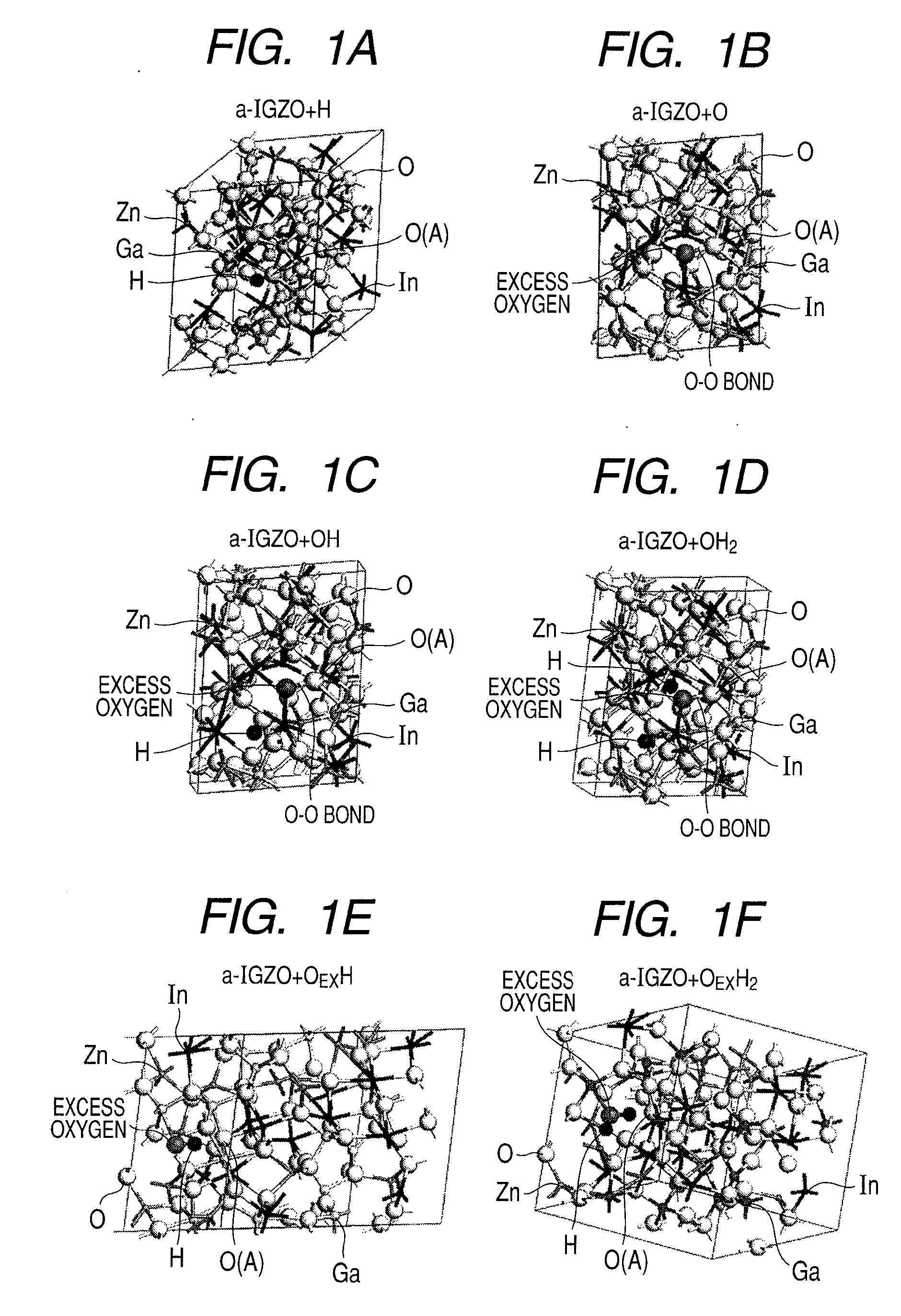
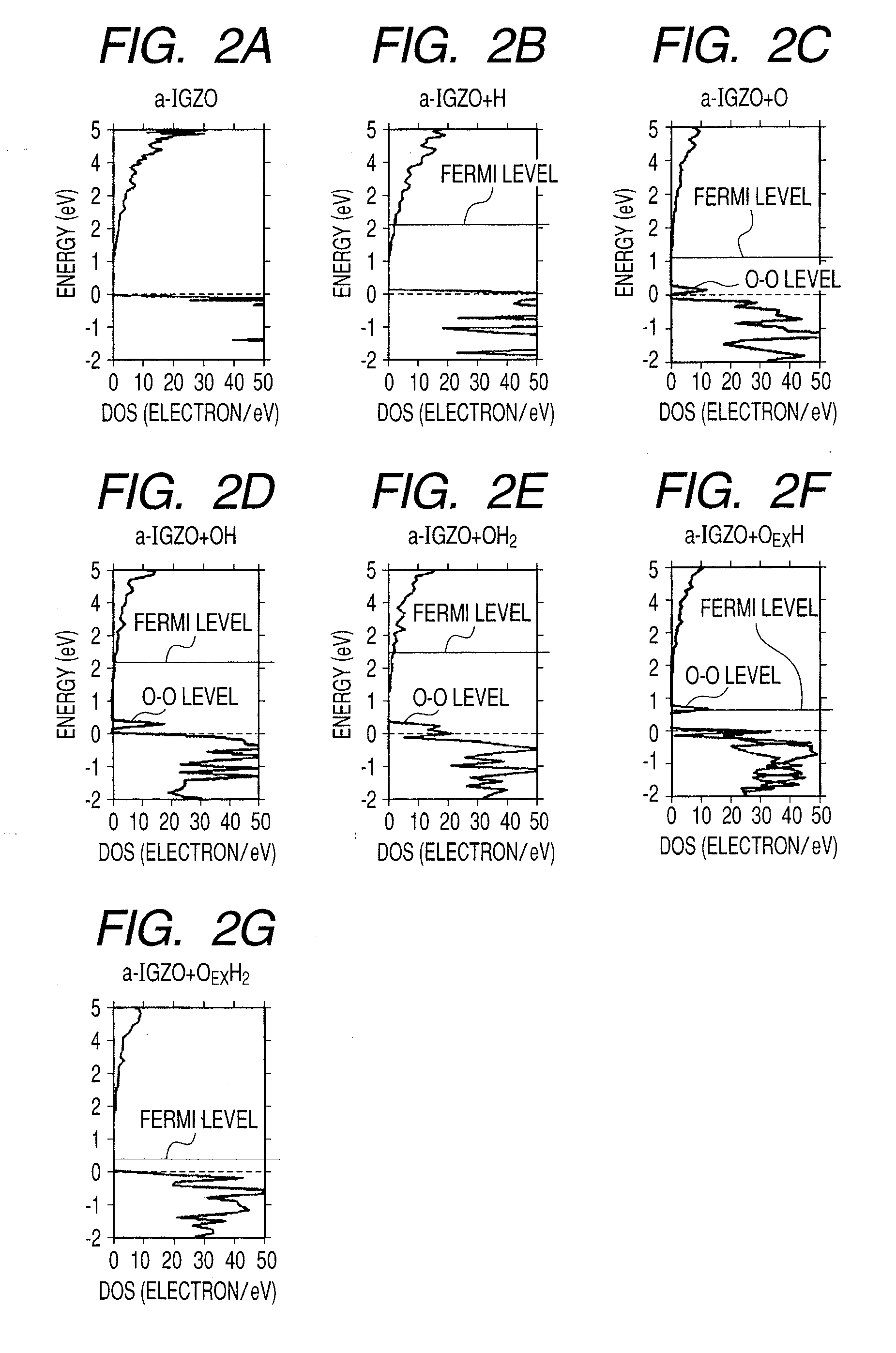
Image

Examples
example 1
[0108]In this example, an embodiment of a TFT device of the present invention is described.
[0109]First, an In—Ga—Zn—O film was formed on a glass substrate as an amorphous oxide semiconductor. The In—Ga—Zn—O film was formed in an argon atmosphere by DC sputtering film formation.
[0110]As a target (material source), a 3-inch sized sintered body having a composition of InGaZnO4 was used, and the applied RF power was 50 W. The distance between the target and the substrate was 60 mm. The In—Ga—Zn—O film was formed in a mixed atmosphere at 5.0×10⁻¹ Pa of argon and water vapor. The partial pressure of the introduced water vapor was 8.0×10⁻⁴ to 6.0×10⁻² Pa. Note that oxygen was not introduced. The substrate temperature at the time of film formation was 25° C.
[0111]With regard to the obtained film, the Hall effect was measured. The result is illustrated in FIG. 3, in which the dependence of the carrier density, the Hall mobility, and the resistivity of the In—Ga—Zn—O film on the partial press...
example 2
[0114]In this example, another embodiment of a TFT device of the present invention is described with reference to FIG. 9.
[0115]First, as a channel layer, an In—Ga—Zn—O film 903 was formed on an n-type low resistance silicon substrate 900 having a thermally grown silicon oxide film 904 at a thickness of 100 nm formed thereon. By DC sputtering in an argon atmosphere, the In—Ga—Zn—O film was formed.
[0116]As the target (material source), a 3-inch sized sintered body having a composition of InGaZnO4 was used, and the applied RF power was 50 W. The distance between the target and the substrate was 60 mm. The In—Ga—Zn—O film was formed in an atmosphere of argon-water vapor mixed gas at 5.0×10⁻¹ Pa with the partial pressure of the introduced water vapor being 6.2×10⁻² Pa. It is to be noted that oxygen was not introduced. The temperature of the substrate when the film was formed was 25° C. The thickness of the amorphous InGaZnO4 channel layer was 30 nm. After that, the channel layer was patt...
example 3
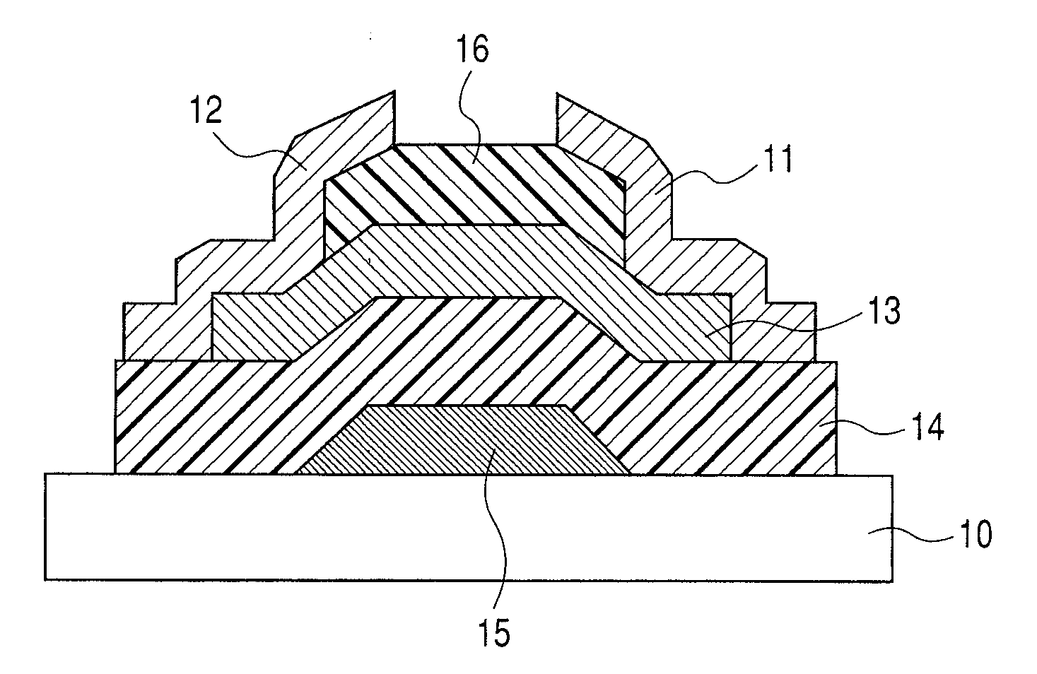
[0118]In this example, another embodiment of a TFT device of the present invention is described with reference to FIG. 4.
[0119]First, an Mo electrode as a gate electrode was formed on a glass substrate 10 by sputtering. Then, patterning was carried out by photolithography. After an SiO2 film as a gate insulating film 14 was formed by sputtering, a source electrode 12 and a drain electrode 11 were formed. Then, similarly to the case of Example 2, an In—Ga—Zn—O film was formed thereon as a channel layer 13. The thickness of the amorphous InGaZnO4 channel layer was 30 nm. The partial pressure of the introduced water vapor was 1.6×10⁻² Pa, 6.2×10⁻² Pa, and 8.6×10⁻² Pa. It is to be noted that oxygen was not introduced. The temperature of the substrate when the film was formed was 25° C.
[0120]Further, an SiO2 film as a protective film 16 was deposited thereon at a thickness of 100 nm by sputtering.
[0121]In this example, the applied RF power was 300 W. The atmosphere at the time of film fo...
PUM
 Abstract
Description
Claims
Application Information