

Plating apparatus and plating method
a technology of plating apparatus and plating method, which is applied in the direction of coating, electric circuit, manufacturing tools, etc., can solve the problems of increasing cost, increasing cost, and in-plane uniformity of a plated film thickness tend to become worse, and achieves good in-plane uniformity and easy alignment
- Summary
- Abstract
- Description
- Claims
- Application Information
AI Technical Summary
Benefits of technology
Problems solved by technology
Method used
Image

Examples
Embodiment Construction
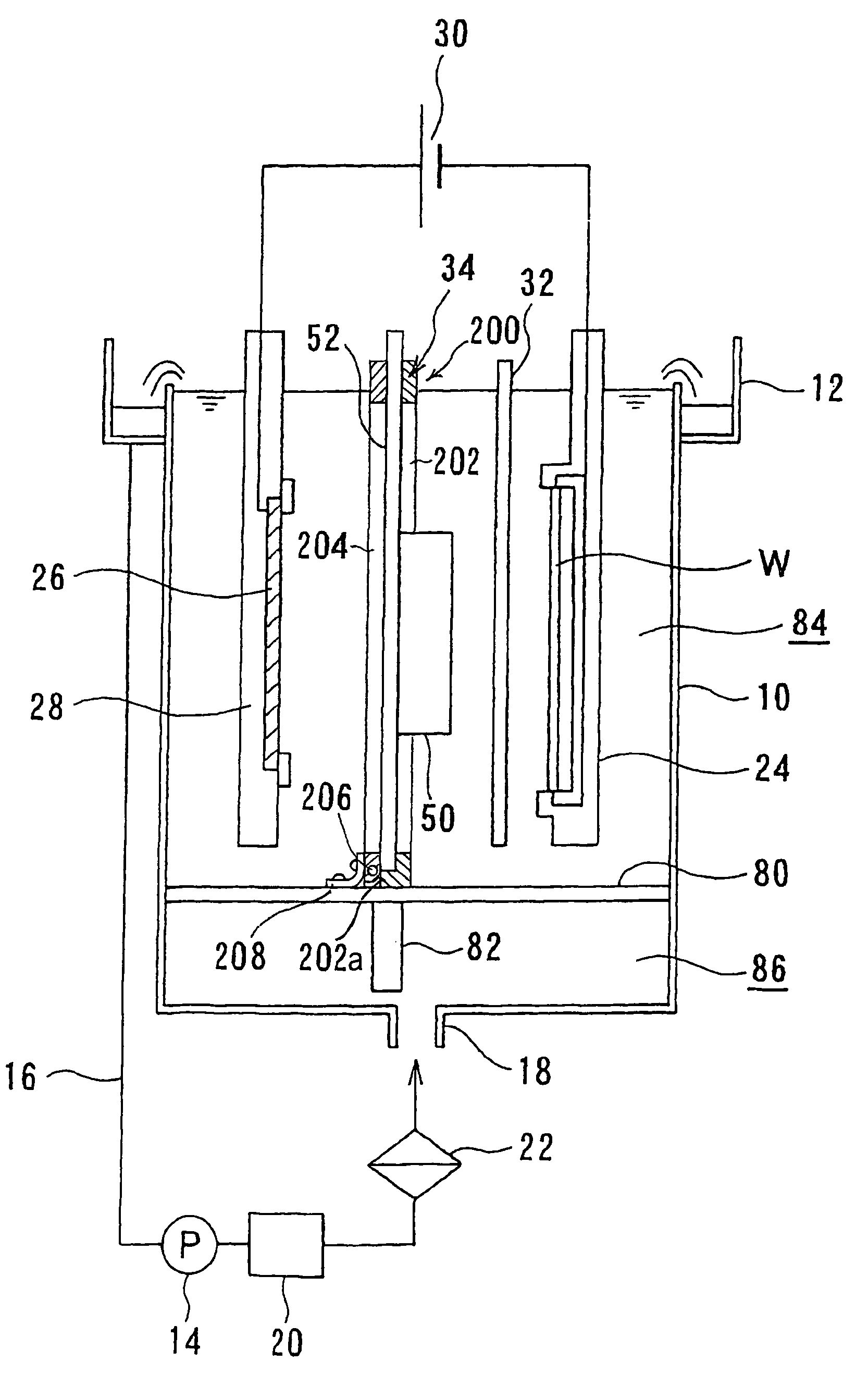
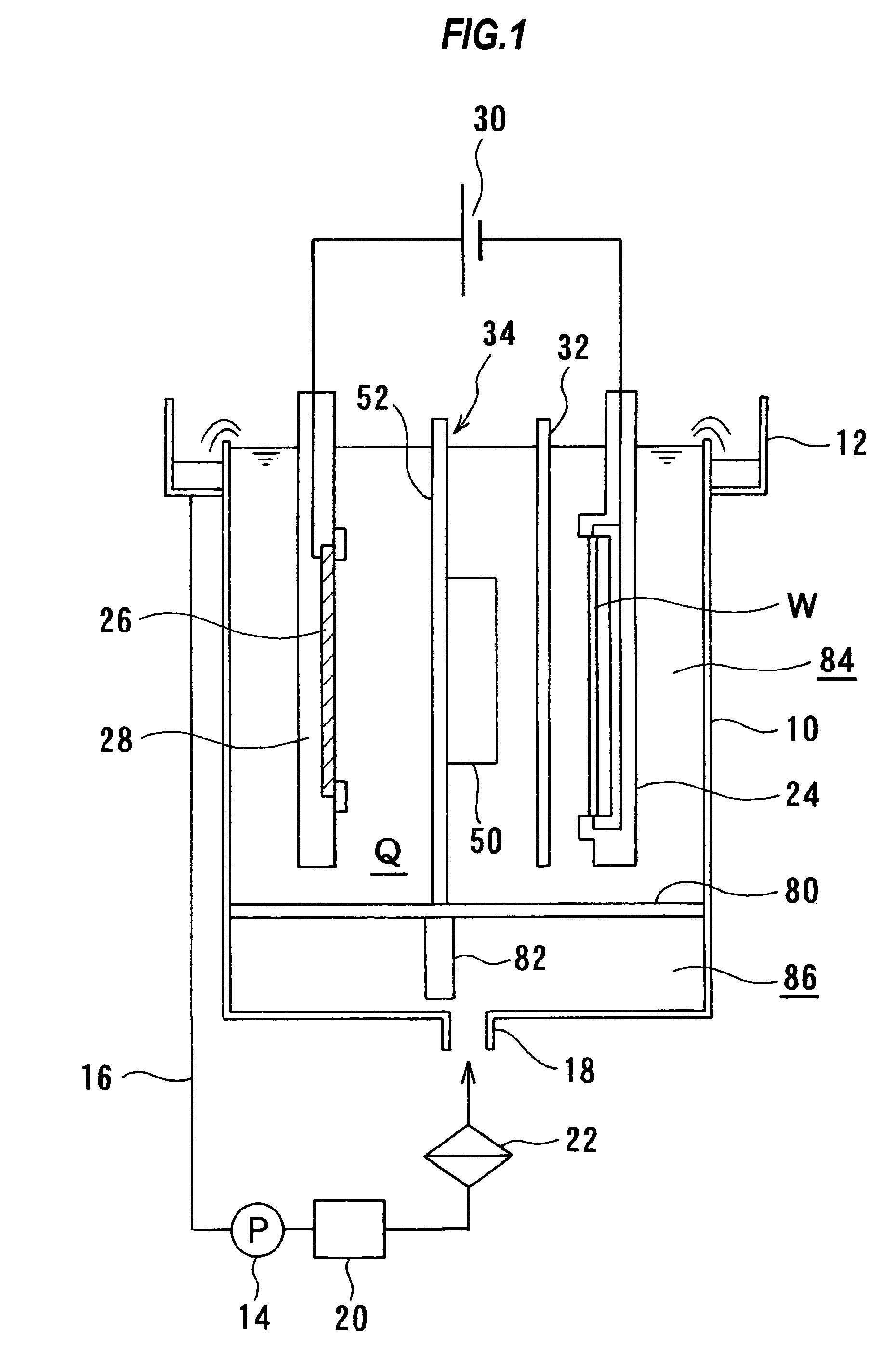
[0102]Preferred embodiments of the present invention will now be described with reference to the drawings. The following description illustrates the case of carrying out copper plating on a surface of a substrate as a plating object. In the following description, the same or equivalent members are given the same reference numerals, and a duplicate description thereof will be omitted.
[0103]FIG. 1 is a vertical sectional front view of a plating apparatus according to an embodiment of the present invention. As shown in FIG. 1, the plating apparatus includes a plating tank 10 holding a plating solution Q therein. An overflow tank 12 for receiving the plating solution Q that has overflowed an edge of the plating tank 10 is provided around an upper end of the plating tank 10. One end of a plating solution supply route 16, which is provided with a pump 14, is connected to a bottom of the overflow tank 12, and the other end of the plating solution supply route 16 is connected to a plating s...
PUM
| Property | Measurement | Unit |
|---|---|---|
| velocity | aaaaa | aaaaa |
| thickness | aaaaa | aaaaa |
| width | aaaaa | aaaaa |
Abstract
Description
Claims
Application Information