Wiring board and method of producing the same

a technology of wiring board and wire, which is applied in the manufacture of cables/conductors, printed circuit aspects, and semiconductor/solid-state devices. it can solve the problems of the miniaturization of the wiring, and achieve the effect of hardly affecting the performance of the wiring board

Active Publication Date: 2012-05-22
SHINKO ELECTRIC IND CO LTD
View PDF23 Cites 2 Cited by
  • Summary
  • Abstract
  • Description
  • Claims
  • Application Information

AI Technical Summary

Benefits of technology

[0010]Illustrative aspects of the present invention provide a wiring board and a method of producing the same in which external connection pads that do not hinder miniaturization of wirings, that can maintain the connection reliability of vias, and that hardly cause degradation of the performance of the wiring board are formed in one face of the wiring board.

Problems solved by technology

This configuration hinders miniaturization of wirings.
Therefore, this disadvantage tends to cause the performance of the wiring board to be degraded.

Method used


Image

  • Wiring board and method of producing the same
  • Wiring board and method of producing the same
  • Wiring board and method of producing the same

Examples


example 1

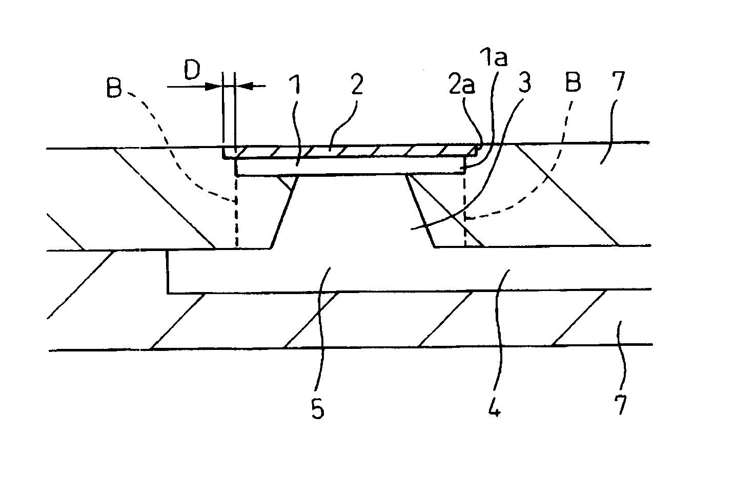
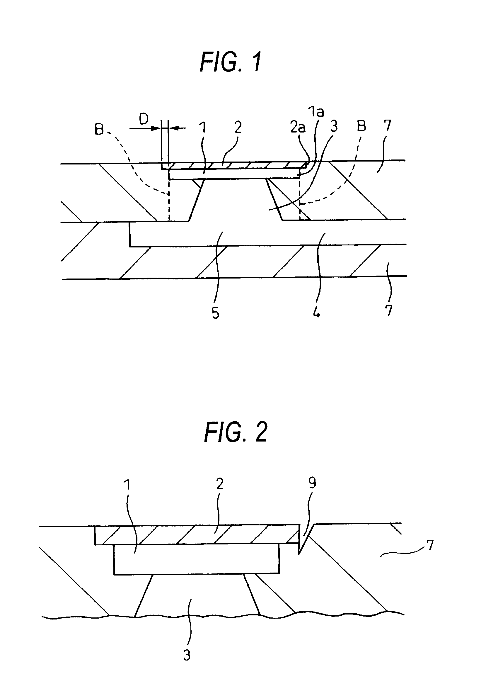
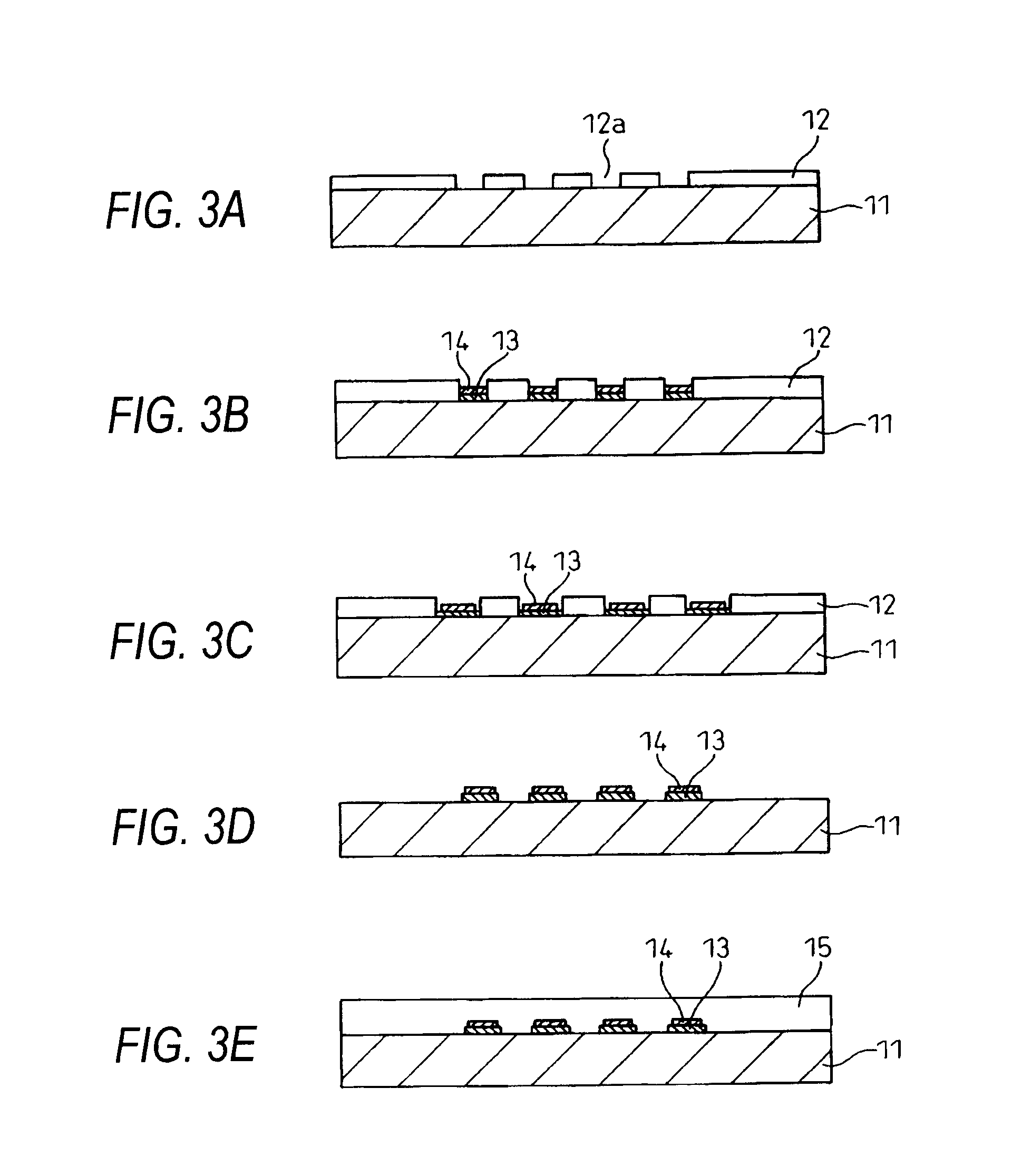
[0054]In Example 1, a wiring board in which the surface of a surface plated layer and that of a wiring board are in the same plane will be described together with a method producing it.

[0055]As shown in FIG. 3A, a plate resist pattern 12 which will be used as a mask pattern is formed on the surface of a Cu plate serving as a support member 11. In FIG. 3A, for the sake of simplicity, only the resist pattern 12 on one face of the support member 11 is shown. Actually, also the opposite face of the support member 11 is covered by a plate resist pattern. As the support member 11, other than a Cu plate, a Cu foil or a plate or foil of another metal or alloy which can be removed by a usual etchant may be used. As shown in FIG. 3B, surface plated layers 13 and external connection pads 14 are sequentially formed by electrolytic plating on the support member 11 which is exposed in bottom portions of opening portions 12a (FIG. 3A) (having a diameter of 100 μm) of the plate resist pattern 12. T...

example 2

[0061]Hereinafter, a wiring board in which the surface of a surface plated layer and that of a wiring board are in the same plane will be described together with another method producing it.

[0062]As shown in FIG. 7A, a plate resist pattern 32 is formed on the surface of a Cu plate serving as a support member 31 (a resist layer (not shown) is formed also on the rear face of the support member 31). As the support member 31, other than a Cu plate, a Cu foil or a plate or foil of another metal or alloy which can be removed by a usual etchant may be used. As shown in FIG. 7B, surface plated layers 33 and external connection pads 34 are sequentially formed by electrolytic plating on the support member 31 which is exposed in bottom portions of opening portions 32a (FIG. 7A) (having a diameter of 100 μm) of the plate resist pattern 32. As each of the surface plated layers 33, an Au layer and Ni layer respectively having thicknesses of 0.5 μm and 5 μm are formed in this sequence. The externa...

example 3

[0067]Hereinafter, an example of a wiring board in which a surface plated layer is positioned in a recess of the wiring board will be described together with a method producing it. The materials and dimensions of the members, the processing methods, and the like used in the following examples are identical with those described in Examples 1 and 2, unless otherwise specified.

[0068]As shown in FIG. 9A, a plate resist pattern 42 having opening portions 42a is formed on the surface of a Cu plate serving as a support member 41 (a resist layer (not shown) is formed also on the rear face of the support member 41). As shown in FIG. 9B, surface plated layers 43 (formed by an Au layer and a Ni layer) and external connection pads 44 made of Cu are sequentially formed by electrolytic plating on the support member 41 which is exposed in bottom portions of opening portions 42a.

[0069]After the plate resist pattern 42 is removed (FIG. 9C), the Cu material is selectively etched so that, as shown in...


PUM


Abstract

A wiring board includes: wiring layers; insulating layers disposed between the wiring layers; and external connection pads respectively including surface plated layers, for connecting to an external circuit. In each of the external connection pads in one face of the wiring board, an outer peripheral edge of the external connection pad is retracted from an outer peripheral edge of the surface plated layer toward a center of the external connection pad.

Description

[0001]This application claims priority from Japanese Patent Application No. 2008-305154, filed on Nov. 28, 2008, the entire contents of which are hereby incorporated by reference.FIELD OF THE INVENTION[0002]The present invention relates to a wiring board and a method of producing the same, and more particularly to a wiring board of a type in which pads for mounting a semiconductor chip or the like are disposed on one face, and pads for connecting with another mounting board are disposed on the other face.DESCRIPTION OF RELATED ART[0003]In a wiring board which is used, for example, in packaging of electronic components such as a semiconductor chip, pads for mounting a semiconductor chip, an electronic component, or the like are disposed on one face, and pads for connecting with another mounting board are disposed on the other face. In order to attain joining with solder bumps which are used for connections with a semiconductor chip or the like, and those with a mounting board, a surf...

Claims


Application Information

Patent Timeline
Patent Type & Authority Patents(United States)
IPC IPC(8): H01L21/44
CPCH01L21/6835H05K1/113H05K3/4682H01L24/16H01L2224/73204H01L2224/32225H01L2224/16225H01L2221/68345H01L2224/16H01L2924/01046H01L2924/01078H01L2924/01079H05K2201/096H05K2201/09845H05K2203/0152H05K2203/0369H05K2203/1184H01L2924/00H01L2924/00014H01L2924/00011H01L2224/0401
Inventor KANEKO, KENTARO
Owner SHINKO ELECTRIC IND CO LTD
Why Eureka
Try Eureka