LED with upstanding nanowire structure and method of producing such

a nanowire and nanowire technology, applied in the direction of instruments, electrical equipment, nanotechnology, etc., can solve the problems of not contributing to the effective luminescence of the device, and achieve the effects of improving the waveguide properties of the nanowire, good waveguide properties, and high doping degr

a nanowire and nanowire technology, applied in the direction of instruments, electrical equipment, nanotechnology, etc., can solve the problems of not contributing to the effective luminescence of the device, and achieve the effects of improving the waveguide properties of the nanowire, good waveguide properties, and high doping degr

US8183587B2Active Publication Date: 2012-05-22QUNANO

Image

  • LED with upstanding nanowire structure and method of producing such
  • LED with upstanding nanowire structure and method of producing such
  • LED with upstanding nanowire structure and method of producing such

Examples


Embodiment Construction

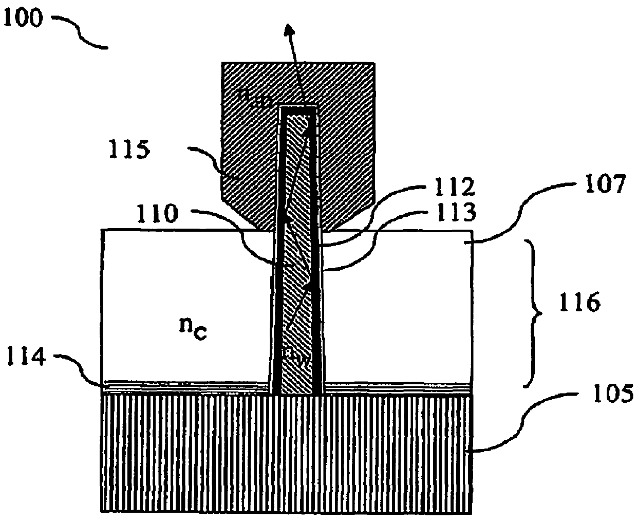
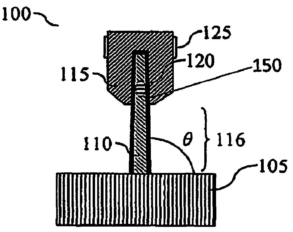
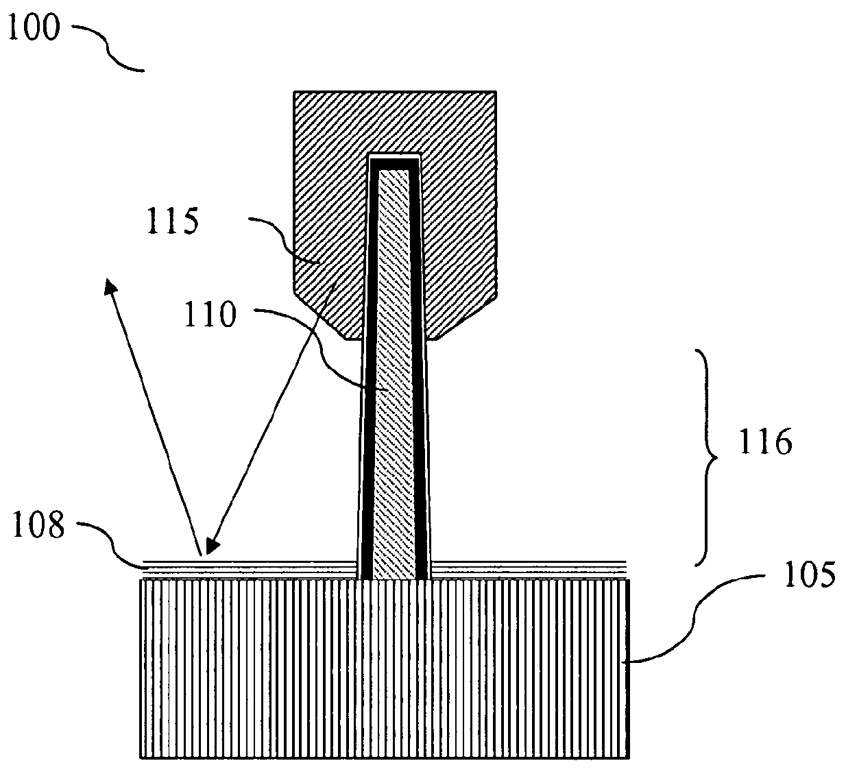
[0029]A nanostructured light emitting diode according to the embodiments of the invention comprises an upstanding nanowire as an active element. Suitable methods for growing nanowires on semiconductor substrates are described in US Published Application 2003 / 010244. Methods of providing epitaxially grown nanowires with heterostructures are to be found in US Published Application 2004 / 0075464.

[0030]For the purpose of this application an upstanding nanowire should be interpreted as a nanowire protruding from the substrate in some angle, the upstanding nanowire for example grown epitaxially from the substrate. The angle with the substrate will typically be a result of the materials in the substrate and the nanowire, the surface of the substrate and growth conditions. By controlling these parameters it is possible to produce nanowires pointing in only one direction, for example vertical, or in a limited set of directions. For example nanowires and substrates of zinc blende and diamond s...


PUM


Abstract

The present invention relates to light emitting diodes, LEDs. In particular the invention relates to a LED comprising a nanowire as an active component. The nanostructured LED according to the embodiments of the invention comprises a substrate and at an upstanding nanowire protruding from the substrate. A pn-junction giving an active region to produce light is present within the structure. The nanowire, or at least a part of the nanowire, forms a wave-guiding section directing at least a portion of the light produced in the active region in a direction given by the nanowire.

Description

TECHNICAL FIELD[0001]The present invention relates to light emitting diodes, LEDs. In particular the invention relates to a LED comprising a nanowire as an active component.BACKGROUND[0002]The majority of present day light emitting diodes (LEDs) are built on planar technology. The PN-junction is constructed as a plurality of layers on a substrate giving a device with an essentially horizontal orientation. The light-producing re-combination takes place in one of the layers. As the layer has a refractive index that is substantially higher than the refractive index of the air, a substantial portion of generated light will be reflected in the layer and not contribute to the effective luminescence of the device. In fact the layer will act as a waveguide in the horizontal plane of the LED. Measures have been suggested to mitigate the effects of the light of LED being trapped in the device and to efficiently extract the light out of the semiconductor layers. Such measures include modifying...

Claims


Application Information

Patent Timeline
22 May 2012
Publication
US8183587B2
IPC
H01L33/00
CPC
B82Y10/00; H01L29/0665; H01L29/0673; H01L29/0676; H01L33/24; H01L33/20; H01L33/08; G02B6/107
Inventors
SAMUELSON, LARS IVAR; PEDERSEN, BO