Memory device and manufacturing method and operating method thereof

a memory device and manufacturing method technology, applied in the direction of semiconductor devices, basic electric elements, electrical appliances, etc., can solve the problems of difficult integration of the eeprom with a general cmos process, disadvantages of the memory device performance, etc., to achieve the effect of reducing the short channel effect and advantageous in the minimization of the memory devi

Active Publication Date: 2012-05-29
MACRONIX INT CO LTD
View PDF19 Cites 1 Cited by
  • Summary
  • Abstract
  • Description
  • Claims
  • Application Information

AI Technical Summary

Benefits of technology

[0011]Accordingly, the present invention is directed to provide a memory device, which can reduce short channel effect and is advantageous in memory device minimization.
[0012]According to another aspect of the present invention, a manufacturing method of a memory device is provided, wherein simple process is used for forming local bit lines, so that the other complex processes can be skipped and defects in the memory can be avoided.
[0013]According to other aspect of the present invention, an operating method of a memory device is provided, which can increase the operation speed of the memory device.
[0021]In the foregoing memory device, the dopant diffusion region under the conductive layers, or the inversion region is used as the source / drain, so that a memory device having shallow junction or non-doped substrate can be formed, which can not only reduce the short channel effect, but also help to minimize the memory device. Besides, with conductive layers as local bit lines, the resistance values of the bit lines can be reduced, and further, the operation speed of the memory device can be increased.
[0032]According to the forgoing manufacturing method of a memory device, simple process is used to form local bit lines (conductive layers), thus, not only the other complex processes are skipped, but also defects in the memory device are avoided. Besides, since it is not necessary to etch the conductive layers at the bottom together in the process of forming the gates, instead, the composite dielectric layer is used as the etching stop layer, thus, incomplete etching, bridging and short circuit between conductive layers are avoided.

Problems solved by technology

These methods will either cause defects in the memory device, or have complex procedure, so that they are very disadvantageous in the manufacturing process.
However, this will cause the resistance values of the buried bit lines 130 being too high, which is very disadvantageous to the performance of the memory device.
However, a floating gate and a controlling gate have to be formed in this EEPROM, so it is difficult to integrate this EEPROM with a general CMOS process, and a silicon oxide layer has to be disposed additionally to separate the floating gate and the bit lines.

Method used


Image

  • Memory device and manufacturing method and operating method thereof
  • Memory device and manufacturing method and operating method thereof
  • Memory device and manufacturing method and operating method thereof

Examples


Embodiment Construction

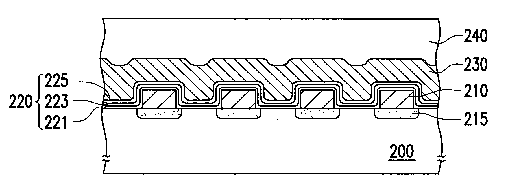
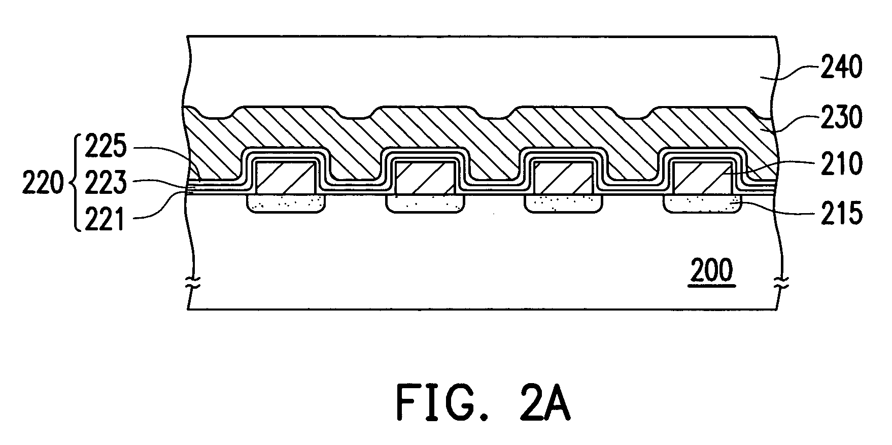
[0068]FIG. 2A is a cross-sectional view of a memory device according to an embodiment of the present invention. Referring to FIG. 2A, the memory device in the present embodiment includes, for example, a substrate 200, a plurality of conductive layers 210, a composite dielectric layer 220 and a plurality of gates 230. Wherein, the conductive layers 210 are disposed on the substrate. The composite dielectric layer 220 is disposed on the substrate 200 and covers the conductive layers 210. The gates 230 are disposed, for example, on the composite dielectric layer 220 and across the conductive layers 210.

[0069]Wherein, the substrate 200 is, for example, p-type silicon substrate. The material of the conductive layers 210 is, for example, doped polysilicon, and the dopant in the doped polysilicon is, for example, n-type dopant such as arsenic and phosphorus. The dopant diffuses, for example, from the conductive layers 210 downwards to the substrate 200 so as to form a dopant diffusion regi...


PUM

PropertyMeasurementUnit
drain voltageaaaaaaaaaa

Abstract

A memory device including a substrate, a plurality of conductive layers, a composite dielectric layer and a plurality of gates are provided. Wherein, the conductive layers are disposed on the substrate. The composite dielectric layer is disposed on the substrate and covers the conductive layers. The composite dielectric layer includes a charge trapping layer. The gates are disposed on the composite dielectric layer and across the conductive layers. Wherein, the conductive layers can be used as local bit lines to reduce the resistance values and improve the performance of the memory device.

Description

BACKGROUND OF THE INVENTION[0001]1. Field of Invention[0002]The present invention relates to a semiconductor device and the method for manufacturing and operating the same, and more particularly to a memory device and the method for manufacturing and operating the same.[0003]2. Description of Related Art[0004]Non-volatile memory is a kind of memory device that the data stored therein will not be lost when the power supply is cut off, which includes such non-volatile memories that data programming, reading, and erasing operations can be performed thereto repeatedly, for example, “Electrically Erasable Programmable Read-Only Memory” (EEPROM) and “silicon Nitride Read-Only Memory”, and such non-volatile memories have been applied widely into various personal computers and electronic devices.[0005]FIG. 1A is a top view of a conventional Nitride Read-Only Memory. FIG. 1B is a cross-sectional view of the cut along line I-I′ of FIG. 1A. Referring to FIGS. 1A and 1B, to manufacture this Nit...

Claims


Application Information

Patent Timeline
Patent Type & Authority Patents(United States)
IPC IPC(8): H01L29/792
CPCH01L27/115H01L27/11568H10B43/30H10B69/00H10B43/10
Inventor LIU, CHENG-JYEHSIUNG, TAI-LIANG
Owner MACRONIX INT CO LTD
Why Eureka
Try Eureka