
Silicone resin composition for optical semiconductor devices and an optical semiconductor device

a technology of optical semiconductors and silicon resins, applied in the direction of mixing, solid balls, sport apparatus, etc., can solve the problems of insufficient light resistance of the composition, yellowing problem, low light output, etc., and achieve excellent adhesion and anti-cracking, poor crack resistance, and high stiffness

Active Publication Date: 2012-06-05
SHIN ETSU CHEM CO LTD
View PDF14 Cites 29 Cited by
  • Summary
  • Abstract
  • Description
  • Claims
  • Application Information

AI Technical Summary

Benefits of technology

[0021]The composition of the present invention does not cause distortion in a device when cured, and can provide a cured product which shows excellent adhesion and an anti-cracking property after repeated heating, and is white, heat resistant and light resistant, on account of the combination of organopolysiloxane (F) which has a linear diorganopolysiloxane moiety having a particular length, an organopolysiloxane (G) having a linear diorganopolysiloxane moiety having a particular length and a methoxy group on the ends, and organopolysiloxane (A) which has the branched structure.BRIEF DESCRIPTION ON THE DRAWING
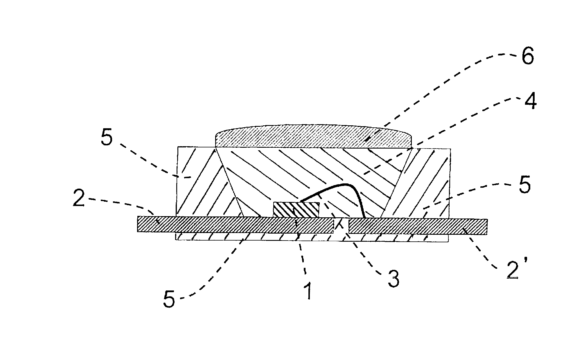
[0022]FIG. 1 is a cross-sectional view which indicates an example of an optical semiconductor device where the silicone resin composition of the present invention is used.BEST MODES OF THE INVENTION(A) Organopolysiloxane
[0023]Organopolysiloxane (A) has a silanol group and forms a cross linked structure in the presence of condensation catalyst (D). In the afore-mentioned average compositional formula (1), R1 is an alkyl group having 1 to 4 carbon atoms and a, b, and c are numbers which satisfy the equations: 0.8<=a<=1.5, 0<=b<=0.3, 0.001<=c<=0.5, and 0.801<=a+b+c<2.
[0024]A composition which comprises an organopolysiloxane with “a” less than the afore-mentioned lower limit, where “a” represents a content of CH3, is not preferred because such a composition provides too hard a cured product, which may crack. If “a” exceeds the afore-mentioned upper limit, such a resin does not solidify. Preferably, “a” satisfies the equation 0.9<=a<=1.2, more preferably 0.9<=a<=1.1.
[0025]If b, content of OR1, exceeds the afore-mentioned upper limit, the molecular weight is so small that crack resistance may be insufficient. Preferably, b satisfies the equation 0.001<=b<=0.2, more preferably 0.01<=b<=0.1. The group, OR1, can be quantified in infrared absorption spectra (IR) or alcohol quantification by alkali cracking.
[0026]If c, content of an OH group bound to an Si atom, exceeds the afore-mentioned upper limit, such an organopolysiloxane gives, after condensation in thermal curing and / or condensation with component (F), a cured product which has a high stiffness, but shows a poor crack resistance. If c is less than the afore-mentioned lower limit, a melting point of the organopolysiloxane tends to be higher, so that problems may occur in workability. If no bond is formed with component (F) and (G), components (F) and (G) are not fixed in a cured product, so that stiffness of the cured product tends to be lower and solvent resistance tends to be bad. Preferably, c satisfies the equation 0.01<=c<=0.3, more preferably 0.05<=c<=0.2. As conditions for controlling c, a complete condensation rate of the alkoxy groups of the raw materials is preferably from 86% to 96%. If the rate is less than 86%, a melting point tends to be low, whereas if it exceeds 96%, a melting point tends to be too high.

Problems solved by technology

Recently, their outputs have become higher and their wavelengths have been shorter, which causes a problem that resin materials present near the optical semiconductor elements are degraded due to light to turn yellow, resulting in lower light output.
However, the afore-mentioned composition has the aforesaid yellowing problem, particularly when an optical semiconductor element is turned on at a high temperature or for a long time.
However, light resistance of the composition is insufficient, again.
Meanwhile, recently, sizes of molded package have become bigger, for instance, in Matrix Array Package (MAP) method and, therefore, warpage in curing of an encapsulating resin has become a serious problem.
Large warpage causes various problems in a package transfer step or a package cutting step.
The afore-mentioned compositions are unsatisfactory also in this respect.

Method used


Image

  • Silicone resin composition for optical semiconductor devices and an optical semiconductor device
  • Silicone resin composition for optical semiconductor devices and an optical semiconductor device
  • Silicone resin composition for optical semiconductor devices and an optical semiconductor device

Examples


synthesis example 1

Organopolysiloxane (A)

[0083]To a one-litter flask were added 100 grams of methyltrichlorosilane and 200 grams of toluene. To the resulting mixture, was added dropwise a mixture of 8 grams of water and 60 grams of isopropyl alcohol over 5 to 20 hours while keeping the inner temperature at −5 to 0 degrees C. by cooling the flask in an ice bath. Then, the mixture was heated at a refluxing temperature for 20 minutes with stirring, and cooled to room temperature, to which 12 grams of water were added dropwise at a temperature below 30 degrees C. over 30 minutes and the mixture was stirred for 20 minutes. Further, 25 grams of water were added dropwise and stirred at a temperature of 40 to 45 degrees C. for 60 minutes. Then, 200 grams of water were added and an organic phase was separated. The organic phase was washed until the phase became neutral and then subjected to azeotropic dehydration, filtration, and strip under reduced pressure to obtain 36.0 grams of a colorless and transparent ...

synthesis example 2

Organopolysiloxane (F)

[0089]5.4 Grams (0.03 mole) of phenylmethyldichlorosilane, 114 grams (0.539 mole) of phenyltrichlorosilane, 100 grams (0.066 mole) of a silicone oil having 20 Si atoms and chlorodimethyl groups on both ends and represented by Cl(Me)2SiO(Me2SiO)nSi (Me)2Cl wherein n is 18 on average, 3000 grams of toluene were mixed, added dropwise to 11000 grams of water, and hydrolyzed at a temperature of 30 to 50 degrees C. for 1 hour. Then, the mixture was aged at 50 degrees C. for 1 hour, to which water was added for washing. Then, the organic phase was subjected to azeotropic dehydration, filtration, and strip under reduced pressure to obtain colorless and transparent organopolysiloxane (F) which had a melt viscosity of 5 Pa·s at 150 degrees C. and is represented by the following formula (9). The content of the silanol group was 3 mole %.

[0090]

(G) Linear Diorganopolysiloxane

[0091]

[0092]n=900 to 1000, ex Shin-Etsu Chemical Co., Ltd.

Additives

[0093](H) Silane coupling agent: ...


PUM

PropertyMeasurementUnit
particle diameteraaaaaaaaaa
reflectanceaaaaaaaaaa
particle diameteraaaaaaaaaa

Abstract

Silicone resin composition for optical semiconductor devices, providing cured product wherein warpage in the devices is reduced and whiteness, heat-resistance, and light resistance are improved. The composition comprises: (A) an organopolysiloxane of the formula(CH3)aSi(OR1)b(OH)cO(4-a-b-c) / 2  (1)wherein R1 is monovalent hydrocarbon and a, b, and c are numbers such that: 0.8<=a<=1.5, 0<=b<=0.3, 0.001<=c<=0.5, and 0.801<=a+b+c<2; (B) white pigment; (C) an inorganic filler other than the white pigment; (D) condensation catalyst; (E) an epoxy resin derived from isocyanuric acid; (F) an organopolysiloxane comprising unit R2SiO and unit RSiO1.5, wherein R is hydroxyl, methyl, ethyl, propyl, cyclohexyl, phenyl, vinyl, or allyl; and(G) a linear diorganopolysiloxane of the formulawherein R5 and R6 are alkyl, cyclohexyl, vinyl, phenyl, or allyl and n is an integer from 800 to 1200.

Description

CROSS REFERENCE[0001]This application claims the benefits of Japanese Patent Application No. 2009-107101 filed on Apr. 24, 2009, the contents of which are herein incorporated by reference.FIELD OF THE INVENTION[0002]The present invention relates to a silicone resin composition for optical semiconductor devices, specifically to a silicone resin composition comprising an organopolysiloxane having a silanol group and an organopolysiloxane having a linear diorganopolysiloxane moiety with a particular length, whereby moldability is good and problems, such as warpage of a semiconductor device in curing and discoloration, particularly yellowing, of a cured product due to light degradation, are markedly reduced.BACKGROUND OF THE INVENTION[0003]Optical semiconductor elements, such as light emitting diodes (LED), are used as indicators or light sources. Recently, their outputs have become higher and their wavelengths have been shorter, which causes a problem that resin materials present near ...

Claims


Application Information

Patent Timeline
Patent Type & Authority Patents(United States)
IPC IPC(8): C08K3/22
CPCC08L83/04H01L21/02126H01L21/02216H01L21/3122H01L23/296C08L83/00C08G77/16H01L2224/48091C08G77/20C08G77/70C08K3/22C08L2205/035H01L33/56H01L2224/29499H01L2224/48247C08G77/18C08L2666/22C08L2666/14C08L2666/54H01L2924/00014
Inventor TAGUCHI, YUSUKEHAGIWARA, KENJISAWADA, JUNICHI
Owner SHIN ETSU CHEM CO LTD
Learn More