

Semiconductor surface modification
a technology of semiconductor materials and surface modifications, applied in the direction of semiconductor/solid-state device testing/measurement, sustainable manufacturing/processing, instruments, etc., can solve the problems of beam path interference, process by-product contamination, and consumption of dopant fluid, so as to improve efficiency and reliability.
Active Publication Date: 2012-06-26
SIONYX
View PDF21 Cites 33 Cited by
- Summary
- Abstract
- Description
- Claims
- Application Information
AI Technical Summary
Benefits of technology
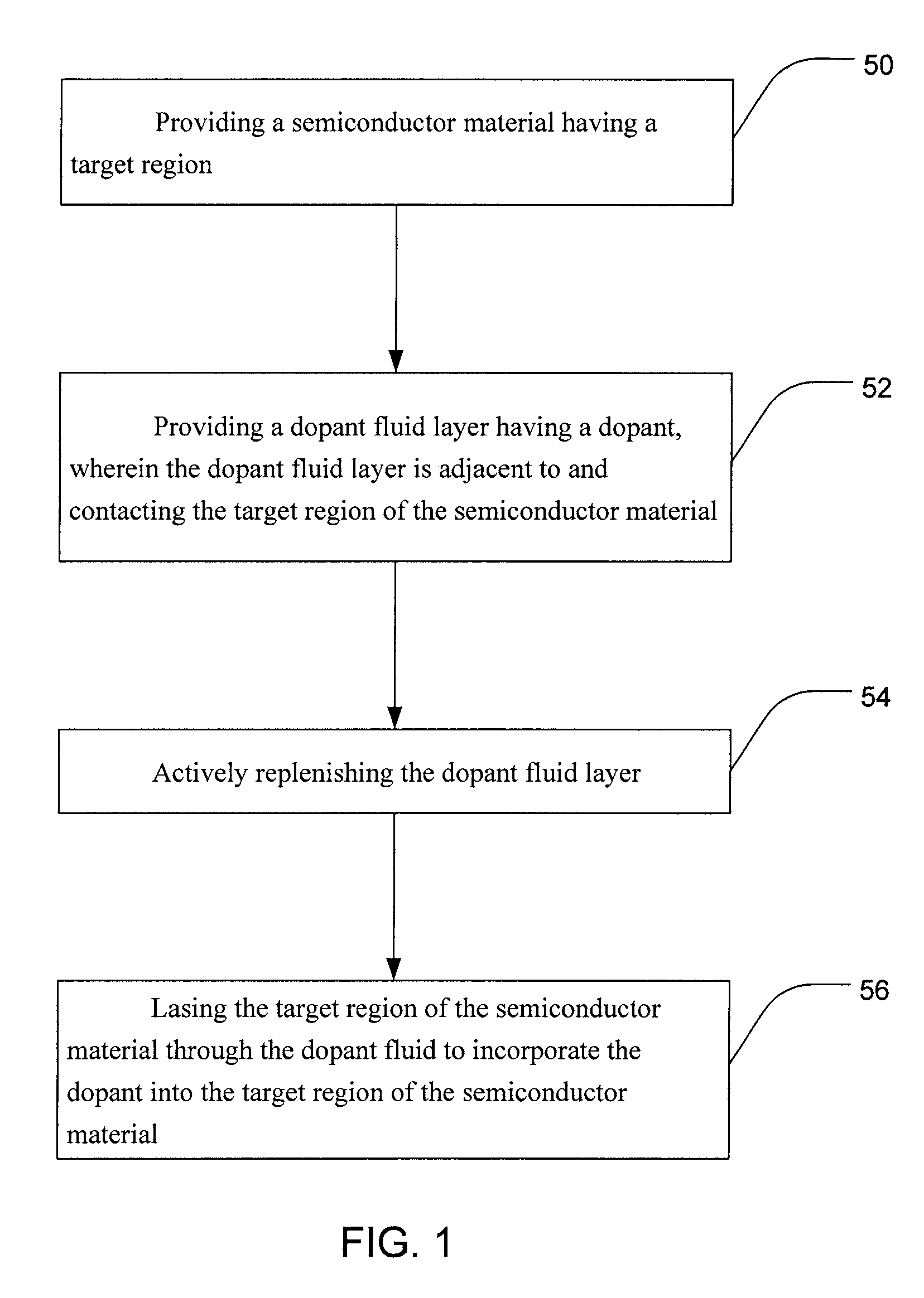
The present invention provides systems and methods for doping and surface-modifying semiconductor materials with enhanced efficiency and reliability. The method involves providing a semiconductor material with a target region and a dopant fluid layer containing a dopant, adjacent to the target region. The dopant fluid layer is actively replenished during the doping process. The system includes a support surface, a dopant fluid input system, and a laser. The dopant fluid input system regulates the dopant fluid layer over the target region of the semiconductor material, while the laser lases the target region through the dopant fluid layer. The technical effects of the invention include improved efficiency and reliability in the manufacturing process of semiconductor materials, as well as surface-modified semiconductor devices incorporating the same.
Problems solved by technology
However, these techniques and other approaches still suffer from drawbacks such as dopant fluid consumption, contamination by process by-products, beam path interference, inefficient batch processing, manufacturing complexities, and semiconductor substrate size limitations, among others.
Method used
View moreImage
Smart ImageViewing Examples

Examples
example
[0050]A silicon is covered in an SF6 dopant gas (i.e. fluid) layer at a gas concentration of 4.3×10⁻⁴ mol / cm3 is provided at an input port, and is removed at an output port. The surface of the silicon is irradiated with pulsed laser radiation with a center wavelength of 800 nm, pulse duration of 100 fs, repetition rate of 1 kHz, and a fluence of 7 kJ / m2.
Login to View More PUM
 Abstract
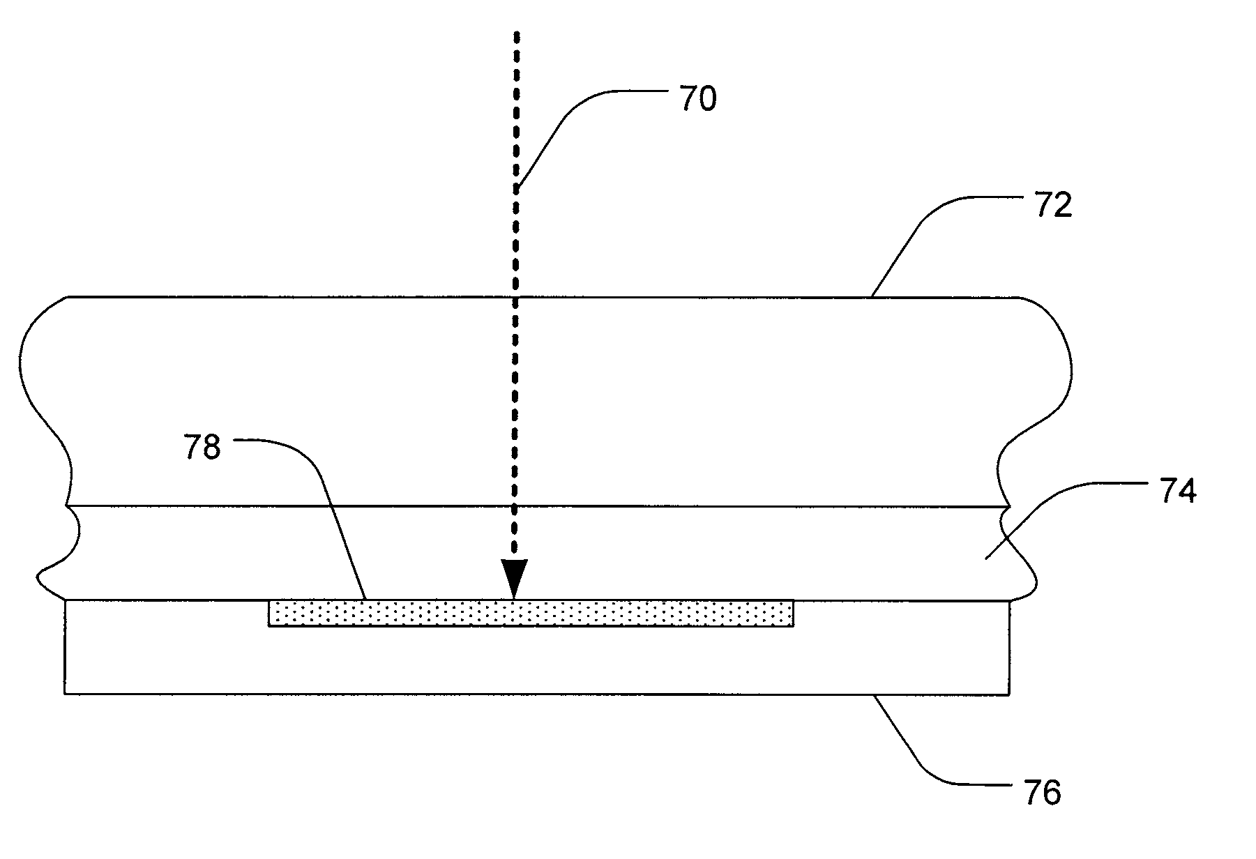
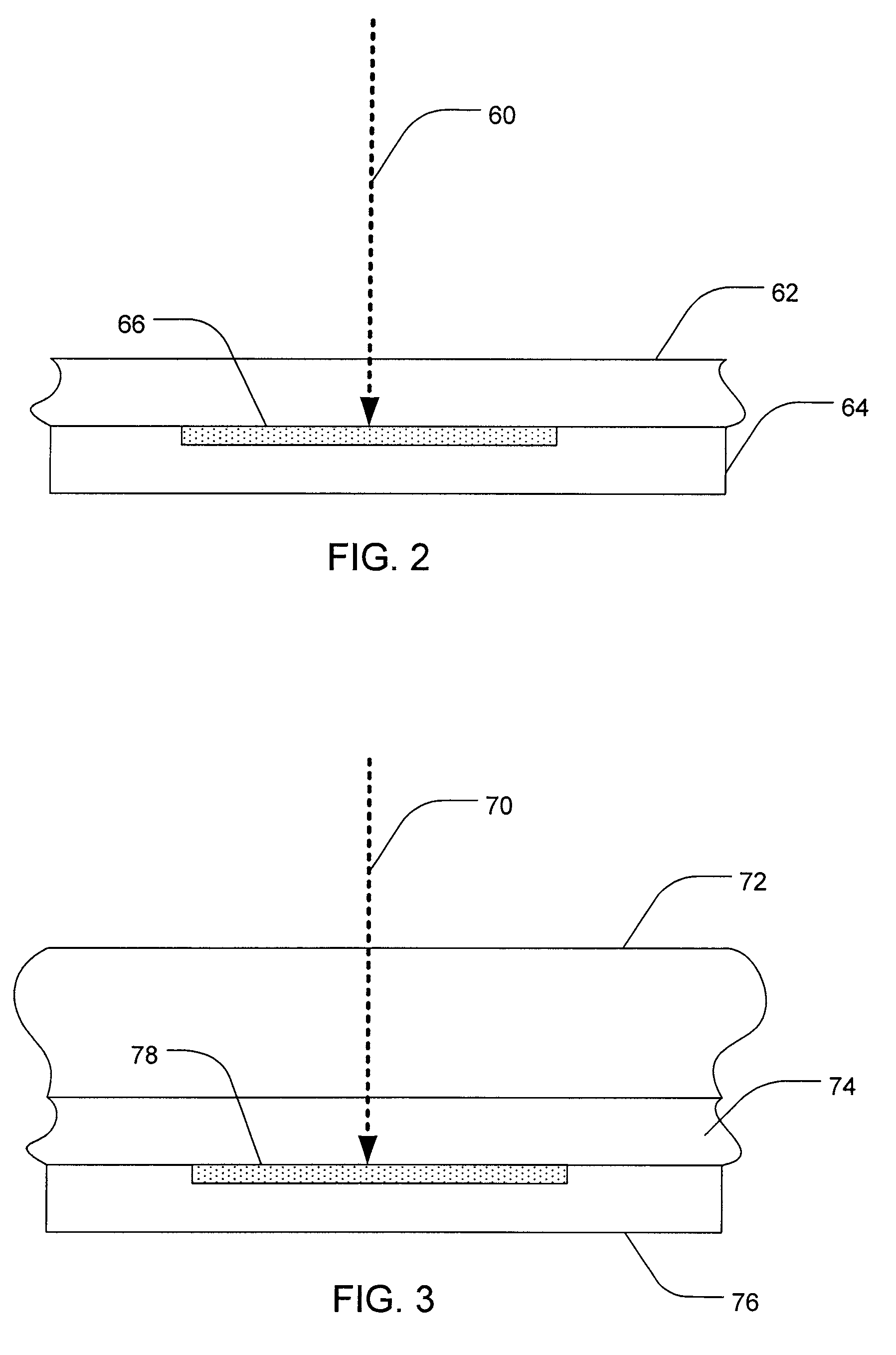
Methods, systems, and devices associated with surface modifying a semiconductor material are taught. One such method includes providing a semiconductor material having a target region and providing a dopant fluid layer that is adjacent to the target region of the semiconductor material, where the dopant fluid layer includes at least one dopant. The target region of the semiconductor material is lased so as to incorporate the dopant or to surface modify the semiconductor material. During the surface modification, the dopant in the dopant fluid layer is actively replenished.
Description
FIELD OF THE INVENTION[0001]The present invention relates generally to systems, methods, and devices for surface-modifying semiconductor materials. Accordingly, the present application involves the fields of physics, chemistry, electricity, and material science.BACKGROUND[0002]Short-pulse laser radiation can be used to create or treat a variety of semiconductor materials in order to enhance their functionality. For example, the properties of silicon photo detectors can be improved and stabilized using short pulse laser radiation treatment. Current techniques for semiconductor surface modification, including doping, using short-pulse laser radiation typically require vacuum evacuation of a sealed chamber containing the material to be surface-modified then filling the chamber with doping fluids or inert fluids so in order to create an environment conducive to the process.[0003]However, these techniques and other approaches still suffer from drawbacks such as dopant fluid consumption, ...
Claims
Login to View More Application Information
Patent Timeline
 Patent Type & AuthorityPatents(United States)
IPC IPC(8): H01L31/101H01L21/66B05C11/10
CPCH01L21/228H01L21/268H01L31/1804Y02E10/547H01L33/005Y10S438/914Y02P70/50
InventorSICKLER, JASONDONALDSON, KEITH
OwnerSIONYX