Semiconductor device and a method of manufacturing the same, and solid-state image pickup element

a semiconductor device and manufacturing method technology, applied in the direction of transistors, television systems, radio control devices, etc., can solve the problems of complicated electronic forming process, and achieve the effects of high yield, high productivity, and increased manufacturing yield

Active Publication Date: 2012-07-03
SONY SEMICON SOLUTIONS CORP
View PDF3 Cites 1 Cited by
  • Summary
  • Abstract
  • Description
  • Claims
  • Application Information

AI Technical Summary

Benefits of technology

[0009]In the manufacture process for the existing solid-state image pickup element composed of only the planer MOS transistors, after a single polycrystalline silicon layer is formed, patterning and ion implantation are carried out by using respective photo masks (each utilizing a photolithography process), thereby forming electrodes of an NMOS portion and electrodes of PMOS portion separately from each other. That is to say, the simple manufacture processes can be adopted in such a manner.
[0055]Moreover, in the vertical MOS transistor having the channel of the first conductivity type, it is possible to increase the concentration of the impurity of the first conductivity type in the portion, of the gate electrode, buried in the inside of the hole. Also, in the planar MOS transistor having the channel of the first conductivity type, it is possible to reduce the concentration of the impurity of the first conductivity type in the gate electrode. As a result, the concentration of the impurity of the gate electrodes of the vertical MOS transistor having the channel of the first conductivity type, and the concentration of the impurity of the planar MOS transistor having the channel of the first conductivity type can be adjusted, thereby making it possible to realize the desired characteristics in the vertical MOS transistor having the channel of the first conductivity type, and the planar MOS transistor having the channel of the first conductivity type.

Problems solved by technology

For this reason, the electrode forming process becomes complicated.

Method used


Image

  • Semiconductor device and a method of manufacturing the same, and solid-state image pickup element
  • Semiconductor device and a method of manufacturing the same, and solid-state image pickup element
  • Semiconductor device and a method of manufacturing the same, and solid-state image pickup element

Examples


Embodiment Construction

[0061]The preferred embodiments of the present invention will be described in detail hereinafter with reference to the accompanying drawings.

[0062]It is noted that the description will be given below in accordance with the following order.

[0063]1. Solid-State Image Pickup Element

[0064]2. Semiconductor Device

[0065]3. Changes

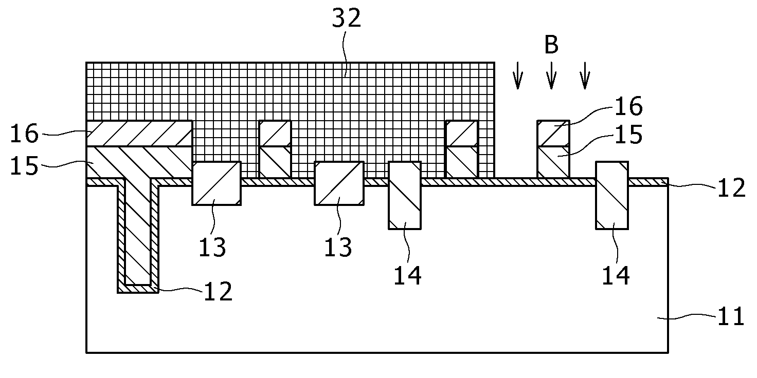
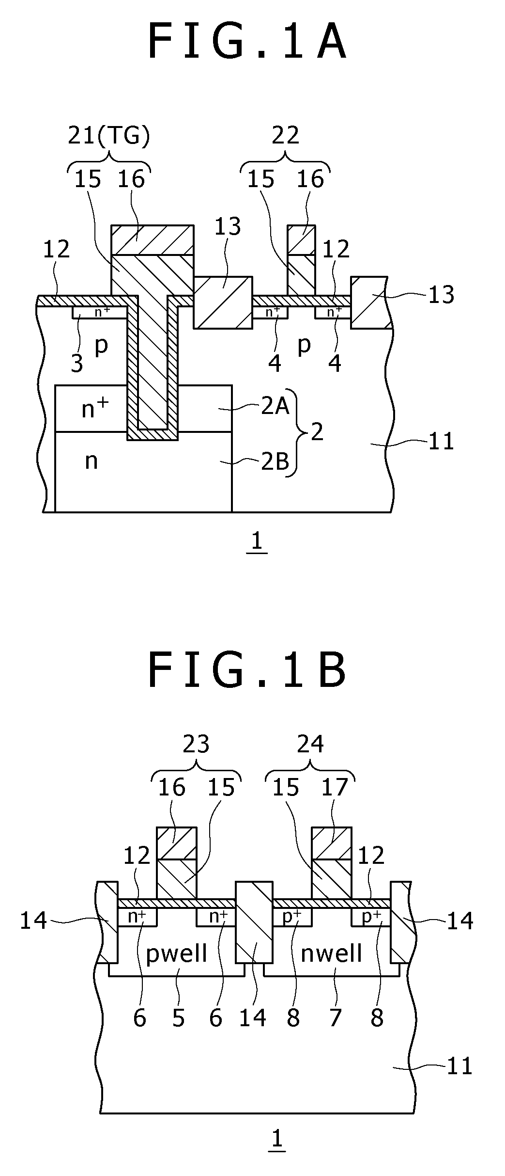
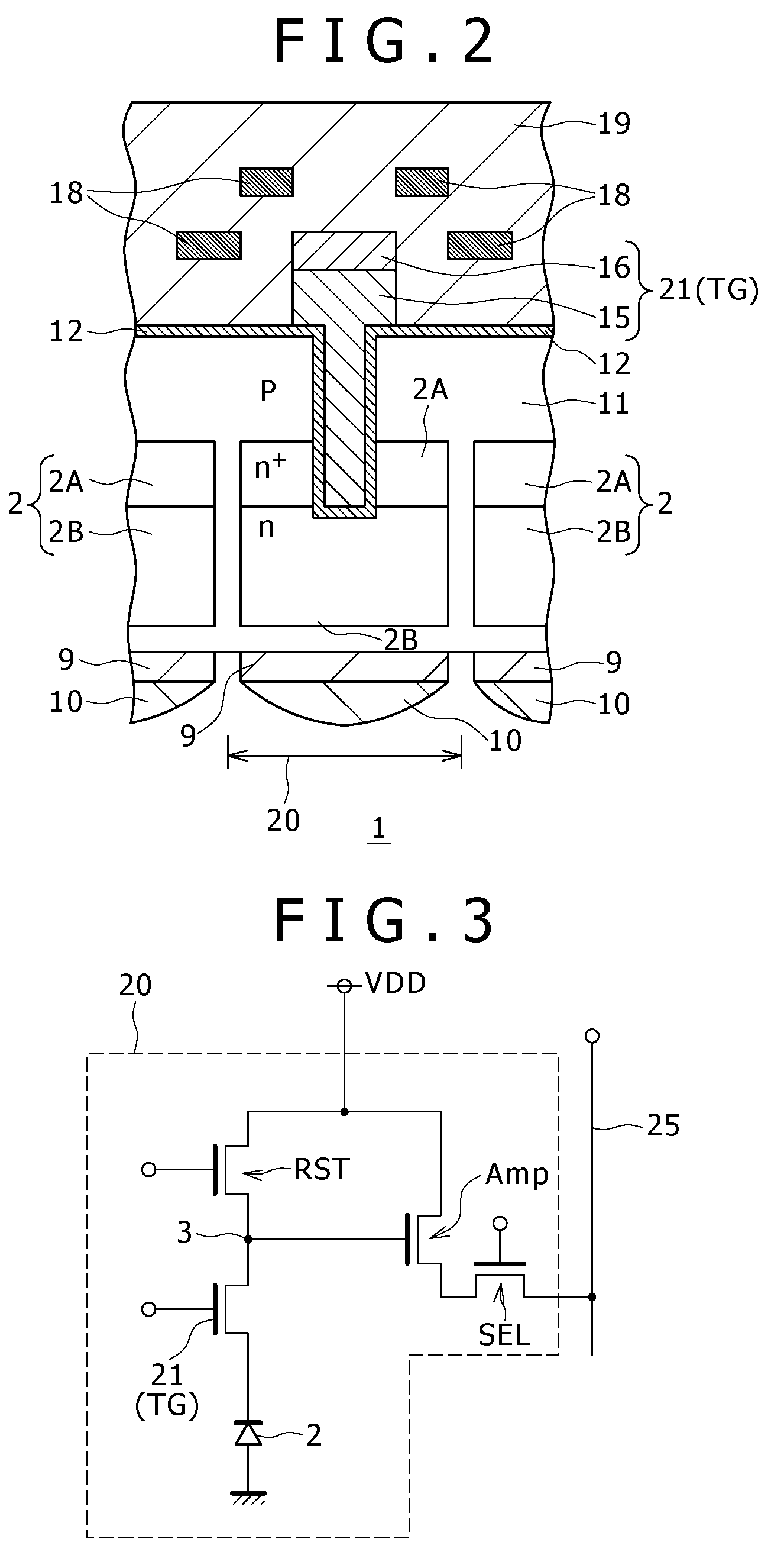
[0066]FIGS. 1A and 1B are respectively a schematic cross sectional view of a pixel portion of a solid-state image pickup element according to an embodiment of the present invention, and a schematic cross sectional view of a logic portion of the solid-state image pickup element according to the embodiment of the present invention. In this embodiment, the present invention is applied to a CMOS solid-state image pickup element (CMOS image sensor).

[0067]The CMOS solid-state image pickup element 1 includes a transfer transistor composed of a vertical NMOS transistor, and another transistor composed of a planar NMOS transistor in a pixel portion, and planar MOS transist...


PUM


Abstract

Disclosed herein is a semiconductor device having a vertical MOS transistor having a channel of a first conductivity type and formed by burying a gate electrode in a semiconductor substrate, a planar MOS transistor having a channel of the first conductivity and having a gate electrode formed on the semiconductor substrate, and a planar MOS transistor having a channel of a second conductivity and having a gate electrode formed on the semiconductor substrate, the semiconductor device, including other circuit element(s), other than a transistor, formed either below or above the vertical MOS transistor having the channel of the first conductivity type.

Description

BACKGROUND OF THE INVENTION[0001]1. Field of the Invention[0002]The present invention relates to a semiconductor device including a vertical metal oxide semiconductor (MOS) transistor having a gate electrode and a gate insulating film which are buried in a semiconductor substrate, and a method of manufacturing the same. In addition, the present invention relates to a solid-state image pickup element including a vertical MOS transistor in a pixel portion.[0003]2. Description of the Related Art[0004]In a solid-state image pickup element, a high integration level for circuits is promoted for enhancement of a sensitivity, and thus there are proposed various kinds of techniques for ensuring an area of a photodiode.[0005]For example, a structure is proposed in which a trench is formed on a photodiode formed on a back surface side of a silicon substrate, and a transfer gate is provided inside the trench, thereby forming a vertical MOS transistor in the trench. This technique, for example, ...

Claims


Application Information

Patent Timeline
Patent Type & Authority Patents(United States)
IPC IPC(8): H01L31/062H01L21/8234H01L27/088H01L27/144H01L27/146H01L29/78H04N5/335H04N5/369H04N5/374
CPCH01L21/823885H01L27/092H01L27/14603H01L27/1464H01L27/14689H01L27/14612H01L27/14609H01L27/14643H01L27/14632
Inventor MANDA, SHUJITAKAHASHI, HIROSHI
Owner SONY SEMICON SOLUTIONS CORP
Why Eureka
Try Eureka