Differential amplifier circuit, display panel driver, and display device

a technology of differential amplifier circuit and display panel, which is applied in the direction of differential amplifiers, amplifiers with semiconductor devices/discharge tubes, instruments, etc., can solve the problems of increasing the difficulty of driving the differential amplifier circuit, and the current consumption amount, etc., to suppress the increase of the current consumption amount and the effect of high slew ra

Inactive Publication Date: 2012-07-17
RENESAS ELECTRONICS CORP
View PDF4 Cites 5 Cited by
  • Summary
  • Abstract
  • Description
  • Claims
  • Application Information

AI Technical Summary

Benefits of technology

[0021]As described above, when the operation state is changed from the steady state to the state that the non-inversion input voltage Vin+ is either higher or lower in level than the inversion input voltage Vin−, the unity gain frequency •u, becomes higher and the second pole frequency |•p2| becomes lower. Therefore, as understood from FIGS. 7A and 7B, the phase margin is reduced. In the differential amplifier circuit shown in FIG. 6 having such characteristics as described above, it is necessary to raise the second pole frequency |•p2| higher in advance in order to prevent the degradation in stability, and therefore a current flowing through the push-pull output stage 5 cannot be reduced in the steady state.
[0025]According to the present invention, it is possible to provide the differential amplifier circuit realizing a high slew rate while suppressing an increase of a current consumption amount.

Problems solved by technology

However, even in the configuration of the differential amplifier circuit shown in FIG. 6, the problem of increasing the current consumption amount cannot be solved.
At this time, in order to avoid the differential amplifier circuit from deviating from a stable operation, it is necessary to feed a large current through the push-pull output stage 5 in advance, and therefore it is difficult to drive the differential amplifier circuit while reducing the current consumption amount.

Method used


Image

  • Differential amplifier circuit, display panel driver, and display device
  • Differential amplifier circuit, display panel driver, and display device
  • Differential amplifier circuit, display panel driver, and display device

Examples


first embodiment

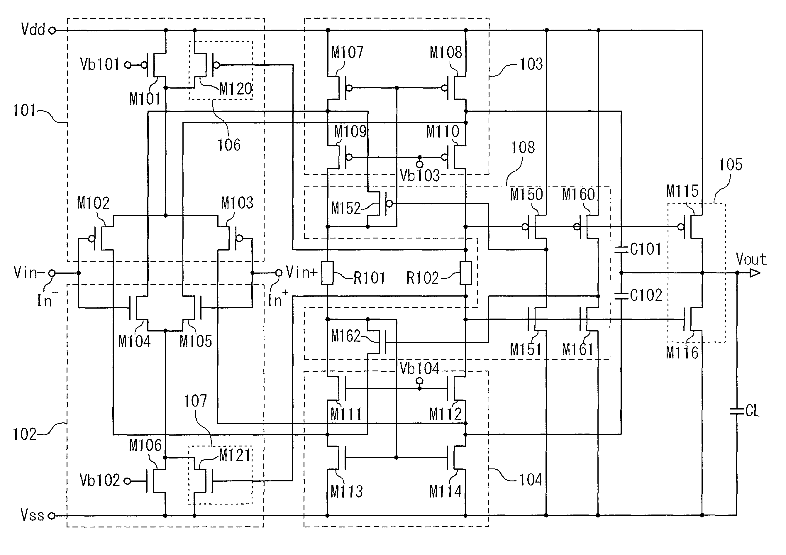
[0034]FIG. 1 is a circuit diagram showing a configuration of a differential amplifier circuit according to a first embodiment of the present invention. The differential amplifier circuit shown in FIG. 1 includes a PMOS differential input section 101, an NMOS differential input section 102, current mirror circuits 103 and 104, resisters R101 and R102, a push-pull output stage 105, a PMOS sub current source 106, an NMOS sub current source 107 and a feedback circuit 108.

[0035]The PMOS differential input section 101 includes PMOS transistors M101, M102 and M103. The PMOS transistors M102 and M103 have their sources connected in common and configure a PMOS differential transistor pair. A gate of the PMOS transistor M102 is connected to a non-inversion input (In−) and a gate of the PMOS transistor M103 is connected to an inversion input (In+). A gate of the PMOS transistor M101 is connected to a bias terminal Vb101 and acts as a constant current source for supplying a bias current to the ...

second embodiment

[0052]FIG. 3 is a circuit diagram showing a configuration of the differential amplifier circuit according to a second embodiment of the present invention. The differential amplifier circuit of the second embodiment has a configuration of adding a PMOS transistor M153 and an NMOS transistor M163 to the feedback circuit 108 in the differential amplifier circuit of the first embodiment shown in FIG. 1. A gate of the PMOS transistor M153 is connected to the commonly connected drains of the PMOS transistor M150 and the NMOS transistor M151, and a drain thereof is connected to a drain of the PMOS transistor M110, and a source thereof is connected to a source of the PMOS transistor M110. A gate of the NMOS transistor M163 is connected to the commonly connected drains of the PMOS transistor M160 and the NMOS transistor M161, and a drain thereof is connected to the drain of a NMOS transistor M112, and the source thereof is connected to a source of the NMOS transistor M112.

[0053]The different...

third embodiment

[0055]FIG. 4 is a circuit diagram showing a configuration of the differential amplifier circuit according to a third embodiment of the present invention. In the differential amplifier circuit of the third embodiment, the configuration of the feedback circuit 108 is modified from those of the first and second embodiments. Specifically, a gate of the NMOS transistor M151 is connected a bias terminal Vb151 instead of a gate of the NMON output transistor M116. A predetermined bias voltage is supplied to the gate of the NMOS transistor M151 through the bias terminal Vb151. Similarly, a gate of the PMOS transistor M160 is connected a bias terminal Vb152 instead of the gate of the PMON output transistor M115. A predetermined bias voltage is supplied to the gate of the PMOS transistor M160 through the bias terminal Vb152. In this case, the NMOS transistor M151 merely acts as a load connected between the PMOS transistor M150 and the negative power source line Vss, and also the PMOS transisto...


PUM


Abstract

A differential amplifying circuit includes first and second differential transistor pairs, first and second constant current sources, first and second current mirror circuits and first and second output transistors. The differential amplifying circuit also includes a feedback circuit configured to perform feed-back operations to the first and second current mirror circuits to restrain reduction of gate voltages of the output transistors. The constant current sources are configured to increase bias currents in response to reduction of the gate voltages of the output transistors.

Description

INCORPORATION BY REFERENCE[0001]This patent application claims a priority on convention based on Japanese Patent Application No. 2010-45256 filed on Mar. 2, 2010. The disclosure thereof is incorporated herein by reference.TECHNICAL FIELD[0002]The present invention relates to a display panel driver provided with a differential amplifier circuit, and a display device.BACKGROUND ART[0003]In recent years, a panel display apparatus such as a liquid crystal display apparatus has been developed to have a finer resolution and a larger screen size, and as a result of this, a source driver for driving the display panel is required to have a capability of driving a large capacitive load at a higher speed. Therefore, it is necessary to improve a slew rate of a differential amplifier circuit used in an output stage of the source driver.[0004]On the other hand, in a market of a cellular phone and other portable equipment with a built-in panel display apparatus, a demand of low current consumption...

Claims


Application Information

Patent Timeline
Patent Type & Authority Patents(United States)
IPC IPC(8): H03F3/45
CPCG02F1/133H03F3/45H03F3/45183H03F3/45219H03F3/4521H03F3/3022
Inventor KATO, FUMIHIKO
Owner RENESAS ELECTRONICS CORP
Why Eureka
Try Eureka