Method and structure of monolithetically integrated inertial sensor using IC foundry-compatible processes

a technology of inertial sensor and monolithecene, which is applied in the direction of microelectromechanical systems, microelectromechanical sensors, semiconductor devices, etc., can solve the problems of limited integration level of mems and cmos, difficult scaling and leverage of capacity and capacity of ic foundries, and superior performance of micromachined sensors. , the effect of reducing parasitics and reducing the size of the chip

Active Publication Date: 2012-07-24
MOVELLA INC
View PDF9 Cites 45 Cited by
  • Summary
  • Abstract
  • Description
  • Claims
  • Application Information

AI Technical Summary

Benefits of technology

[0009]Comparing to the incumbent bulk or surface micromachined MEMS inertial sensors, the vertically monolithically integrated inertial sensors have smaller chip size, lower parasitics, higher sensitivity, lower

Problems solved by technology

In addition, micromachined sensors have superior performance, lower power, and lower cost comparing to macro electromechanical sensors.
The incumbent micromachined inertial technologies, however, are based on ME

Method used


Image

  • Method and structure of monolithetically integrated inertial sensor using IC foundry-compatible processes
  • Method and structure of monolithetically integrated inertial sensor using IC foundry-compatible processes
  • Method and structure of monolithetically integrated inertial sensor using IC foundry-compatible processes

Examples


Embodiment Construction

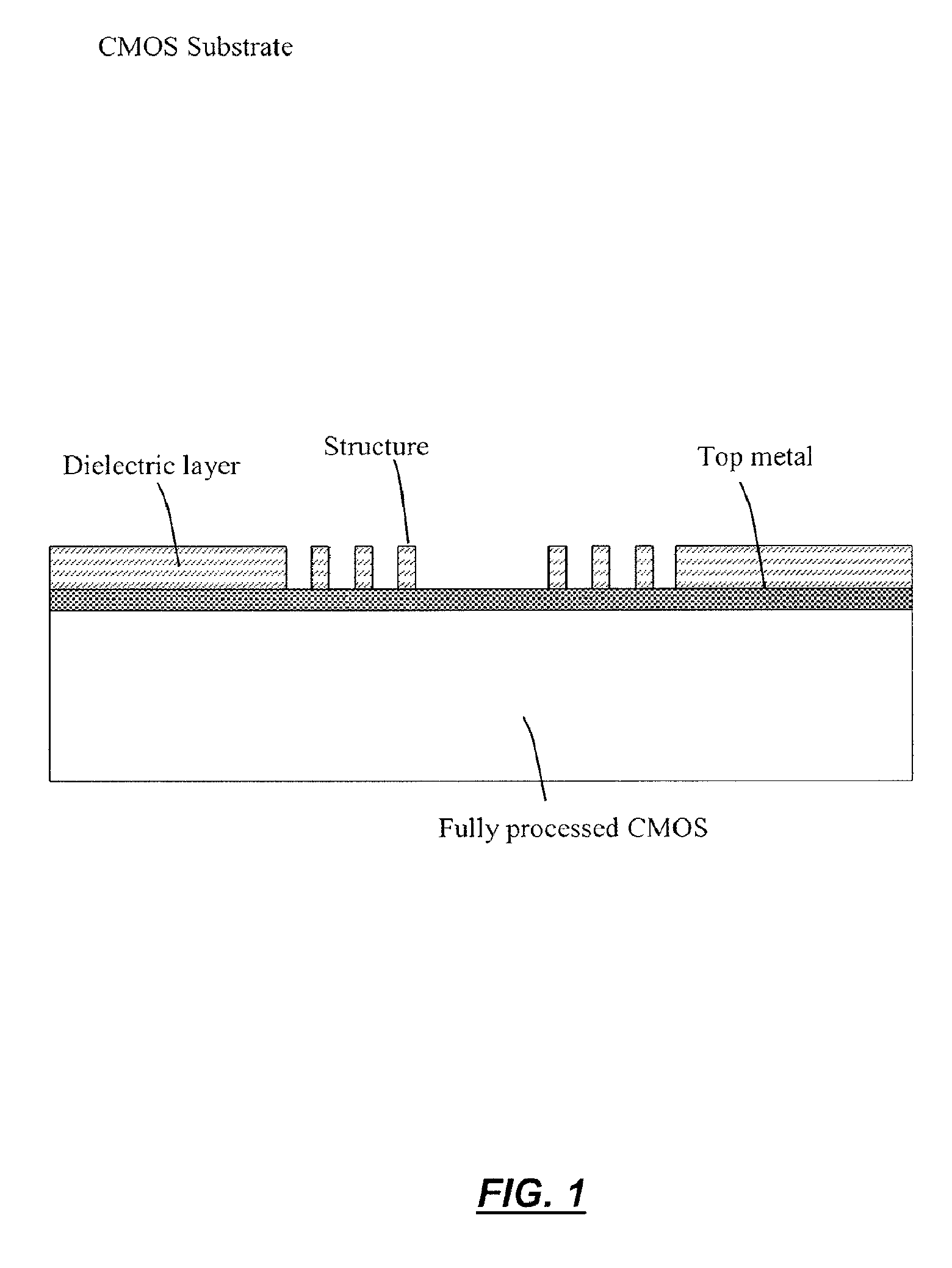
[0030]FIG. 1 is a simplified cross section diagram of components of a starting CMOS substrate according to one embodiment of the present invention. As depicted, the starting substrate is a fully processed CMOS wafer. A dielectric layer such as oxide and nitride is deposited on top of a top metal layer of the CMOS wafer. The dielectric layer is then patterned to form a structure that provides anchor points for stationary members of the mechanical sensing device.

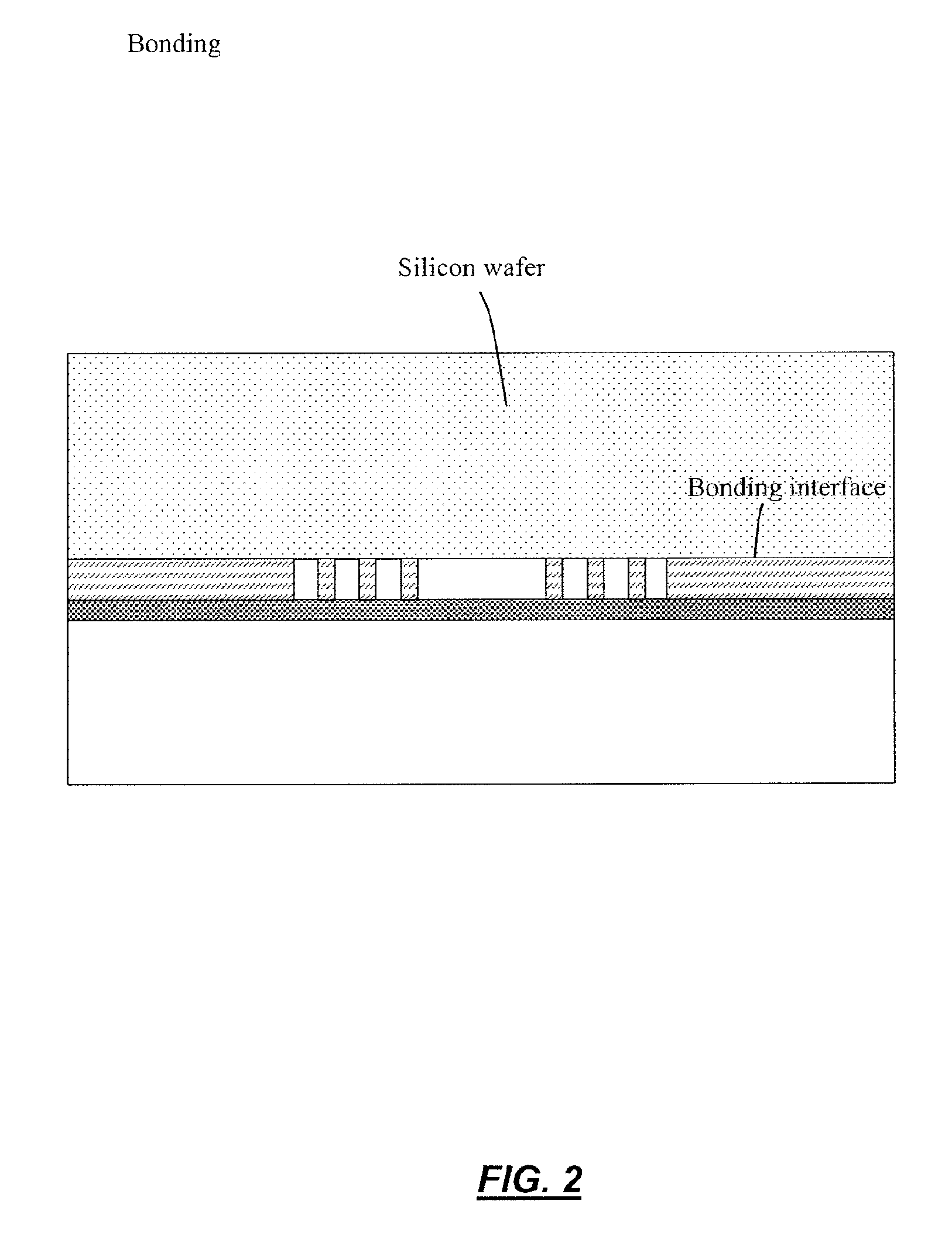
[0031]FIG. 2 is a simplified cross section diagram of components of a monolithically integrated inertial sensing device according to one embodiment of the present invention. As depicted, a silicon wafer is bonded to the CMOS substrate. The bonding methods include but not limited to: covalent, Sprin-on-glass (SOG), Eutectic, and anodic. The bonding temperature is CMOS compatible and below 400 C.

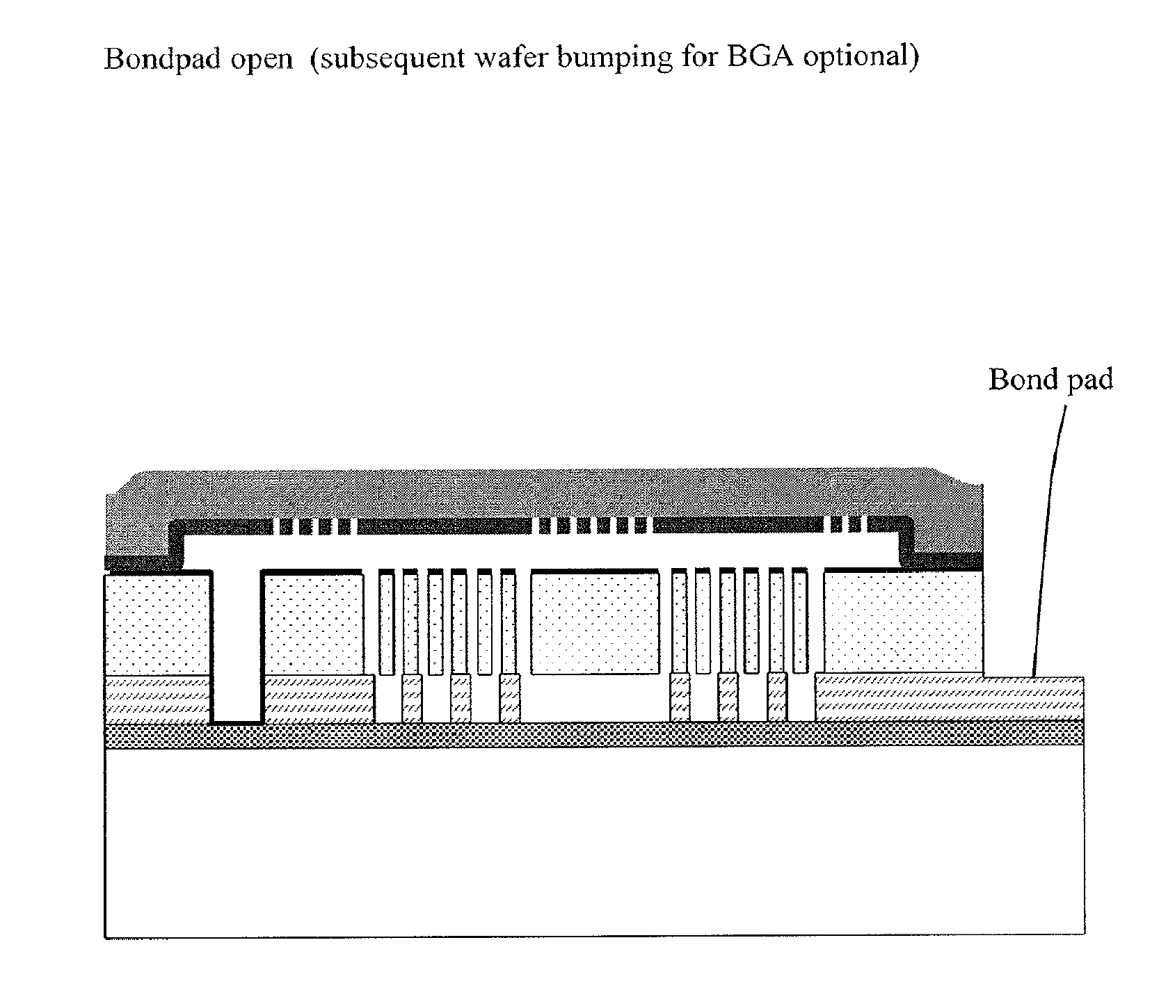
[0032]FIG. 3 is a simplified cross section diagram of components of a monolithically integrated inertial sensing device according to on...


PUM


Abstract

The present invention relates to integrating an inertial mechanical device on top of a CMOS substrate monolithically using IC-foundry compatible processes. The CMOS substrate is completed first using standard IC processes. A thick silicon layer is added on top of the CMOS. A subsequent patterning step defines a mechanical structure for inertial sensing. Finally, the mechanical device is encapsulated by a thick insulating layer at the wafer level. Comparing to the incumbent bulk or surface micromachined MEMS inertial sensors, the vertically monolithically integrated inertial sensors have smaller chip size, lower parasitics, higher sensitivity, lower power, and lower cost.

Description

CROSS-REFERENCES TO RELATED APPLICATIONS[0001]This application is a continuation application of U.S. patent application Ser. No. 12 / 490,067, filed Jun. 23, 2009, which claims priority to and benefit from U.S. Provisional Patent Application No. 61 / 075,726, filed Jun. 25, 2008, both of which are commonly assigned and incorporated herein in their entirety by reference for all purposes.STATEMENT AS TO RIGHTS TO INVENTIONS MADE UNDER FEDERALLY SPONSORED RESEARCH OR DEVELOPMENT[0002]NOT APPLICABLEREFERENCE TO A “SEQUENCE LISTING,” A TABLE, OR A COMPUTER PROGRAM LISTING APPENDIX SUBMITTED ON A COMPACT DISK[0003]NOT APPLICABLEBACKGROUND OF THE INVENTION[0004]The present invention relates generally to monolithic techniques for micromachined technologies and integrated circuits. More particularly, the present invention provides a method and resulting device including both MEMS and integrated circuits using standard foundry compatible processes. Merely by way of example, the invention can be a...

Claims


Application Information

Patent Timeline
IPC IPC(8): H01L21/66
CPCH01L22/12H01L22/26B81C1/0023B81C1/00246H01L27/0688B81B2201/025B81C2203/0145B81C2203/0735
Inventor YANG, XIAO CHARLES
Owner MOVELLA INC
Why Eureka
Try Eureka