Quantum interference device, atomic oscillator and magnetic sensor

a quantum interference and atomic oscillator technology, applied in semiconductor lasers, instruments, horology, etc., can solve the problems of power saving, difficult to reduce laser power, so as to improve the efficiency of laser power use and the efficiency of occurrence of an eit phenomenon in alkali metal atoms

Inactive Publication Date: 2012-10-02
SEIKO EPSON CORP
View PDF4 Cites 7 Cited by
  • Summary
  • Abstract
  • Description
  • Claims
  • Application Information

AI Technical Summary

Benefits of technology

[0008]An advantage of some aspects of the invention is to provide a quantum interference device in which the occurrence efficiency of an EIT phenomenon in alkali metal atoms is raised and the use efficiency of laser power can be improved, and to provide a small atomic oscillator or a magnetic sensor by using this.
[0012]Accordingly, according to this aspect of the invention, the quantum interference device can be provided in which the occurrence efficiency of the EIT phenomenon in the alkali metal atoms is raised, and the use efficiency of the laser power can be improved.

Problems solved by technology

In order to increase the intensity of the EIT signal in the state where the EIT occurrence efficiency is low as described above, the thickness or the height of the cell must be increased as disclosed in the patent document 1, and there is a problem that miniaturization is difficult.
Besides, in the state where the EIT occurrence efficiency is low, since the use efficiency of laser power is low, when the intensity of the EIT signal is kept at a certain level or higher, it is difficult to reduce the laser power, and there is a disadvantage also in power saving.

Method used


Image

  • Quantum interference device, atomic oscillator and magnetic sensor
  • Quantum interference device, atomic oscillator and magnetic sensor
  • Quantum interference device, atomic oscillator and magnetic sensor

Examples


third embodiment

(3) Third Embodiment

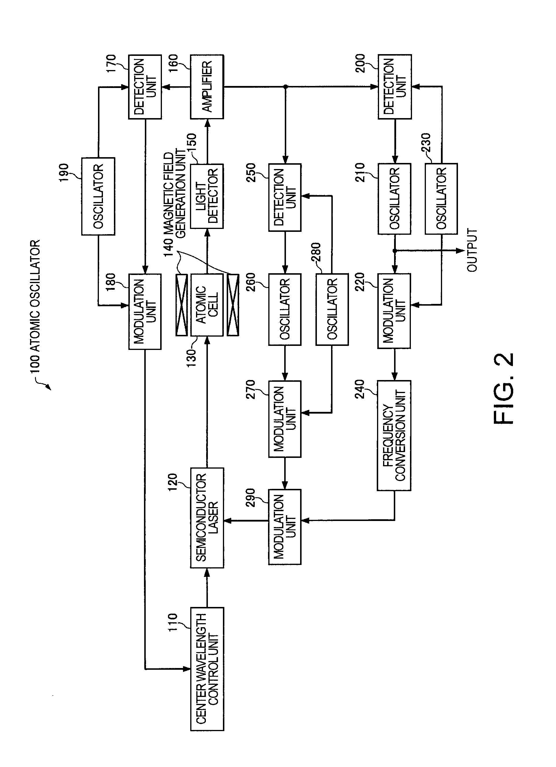
[0092]FIG. 11 is a view showing a structure of an atomic oscillator of a third embodiment using the quantum interference device 1 of FIG. 1. As shown in FIG. 11, the atomic oscillator 100 of the third embodiment is different from the atomic oscillator 100 of the first embodiment shown in FIG. 2 in that the detection unit 250, the oscillator 260, the modulation unit 270 and the oscillator 280 are deleted, and a magnetic field detection unit 330, a frequency setting unit 340, a frequency conversion unit 350 and a magnetic field control unit 360 are newly added. In FIG. 11, the same component as that of FIG. 2 is denoted by the same reference numeral and its description is omitted.

[0093]The magnetic field control unit 360 controls so that the magnetic field generation unit 140 generates a magnetic field of desired intensity. For example, when a magnetic field generation unit 140 is a coil, the magnetic field control unit 360 controls the magnitude of a current flowi...

modified example

[0100]FIG. 12 is a view showing a structure of a modified example of the atomic oscillator 100 of the third embodiment. In an atomic oscillator 100 shown in FIG. 12, the magnetic field detection unit 330 is deleted from the atomic oscillator 100 shown in FIG. 11. Then, a frequency setting unit 340 controls a frequency conversion ratio of a frequency conversion unit 350 based on control information of a magnetic field control unit 360 to a magnetic field generation unit 140. That is, in the atomic oscillator 100 of FIG. 12, the intensity of a magnetic field is estimated based on the control information to the magnetic field generation unit 140, and the conversion ratio of the frequency conversion unit 350 is controlled. Accordingly, although the frequency accuracy of the output signal of the frequency conversion unit 350 is inferior to the oscillator 210 of FIG. 11, the accuracy of Δω has only to be secured to such a degree that alkali metal atoms enclosed in an atomic cell 130 can s...

first embodiment

(1) First Embodiment

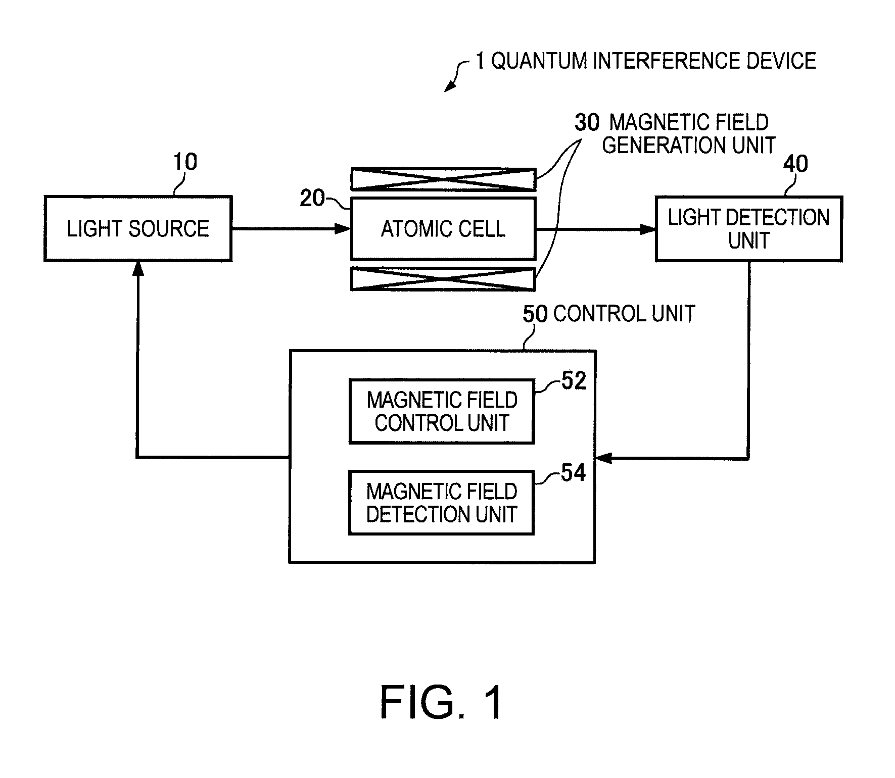
[0101]FIG. 13 is a view showing a structure of a magnetic sensor of a first embodiment using the quantum interference device 1 of FIG. 1. As shown in FIG. 13, the magnetic sensor 400 of the first embodiment has the same structure as that of the atomic oscillator 100 of the first embodiment shown in FIG. 2 except that an oscillation signal of an oscillator 260 becomes an output signal. In FIG. 13, the same component as that of FIG. 2 is denoted by the same reference numeral and its description is omitted.

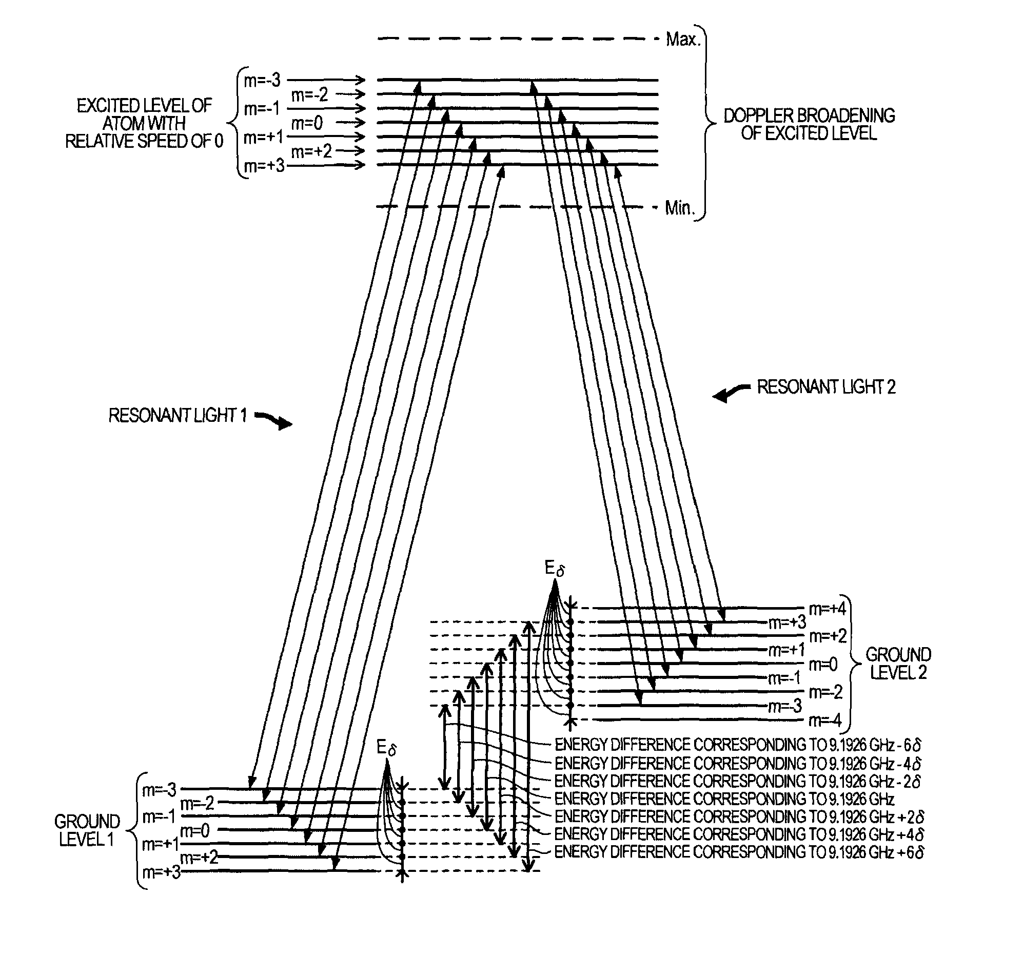
[0102]As described before, when magnetic field is applied to an atomic cell 130, the ground level 1 and the ground level 2 of an alkali metal atom are divided into plural Zeeman split levels different from each other in magnetic quantum number m. In both the ground level 1 and the ground level 2, an energy difference Eδ between two Zeeman split levels different in magnetic quantum number m by one is proportional to the intensity of the magnetic field. According to...


PUM


Abstract

A quantum interference device causing electromagnetically induced transparency in an alkali metal atom includes: a light source generating first and second resonant lights with frequency differences Δω; a magnetic field generator applying a magnetic field to the atom; a light detector detecting intensities of the first and second resonant lights passing through the atom; and a controller causing a frequency difference between specified first and second resonant lights to equal a frequency difference corresponding to an energy difference between two ground levels of the atom based on the detected light. The controller causes the frequency Δω or magnetic field intensity to satisfy 2×δ×n=Δω or Δω×n=2×δ. The frequency δ corresponds to an energy difference between two Zeeman split levels differentiated by one magnetic quantum number and generated in the two ground levels of the atom by energy splitting.

Description

CROSS-REFERENCE TO RELATED APPLICATIONS[0001]The entire disclosure of Japanese Patent Application No. 2009-205643, filed Sep. 7, 2009 is expressly incorporated by reference herein.BACKGROUND[0002]1. Technical Field[0003]The present invention relates to a quantum interference device, an atomic oscillator and a magnetic sensor.[0004]2. Related Art[0005]An atomic oscillator based on an electromagnetically induced transparency (EIT) system (also called a coherent population trapping (CPT) system) is an oscillator using a phenomenon (EIT phenomenon) in which when two resonant lights different from each other in wavelength (frequency) are simultaneously irradiated to an alkali metal atom, the absorption of the two resonant lights is stopped. It is known that the interaction mechanism between the alkali metal atom and the two resonant lights can be explained in a Λ-type 3-level system model. The alkali metal atom has two ground levels, and when resonant light 1 having a wavelength (frequen...

Claims


Application Information

Patent Timeline
Patent Type & Authority Patents(United States)
IPC IPC(8): H01S1/06
CPCG04F5/145H03L7/26H01S5/0687
Inventor AOYAMA, TAKUCHINDO, KOJI
Owner SEIKO EPSON CORP
Why Eureka
Try Eureka