Method for forming silicon nitride film, method for manufacturing nonvolatile semiconductor memory device, nonvolatile semiconductor memory device and plasma apparatus

a semiconductor memory and nonvolatile technology, applied in semiconductor devices, chemical vapor deposition coatings, coatings, etc., can solve the problems of reduced cvd or thermal cvd film, inability to achieve silicon nitride film having inability to achieve a desired trap density, etc., to achieve excellent data storage capacity and excellent data storage capacity

Inactive Publication Date: 2012-11-27
TOKYO ELECTRON LTD
View PDF9 Cites 0 Cited by
  • Summary
  • Abstract
  • Description
  • Claims
  • Application Information

AI Technical Summary

Benefits of technology

[0007]It is therefore an object of the present invention to provide a silicon nitride film-forming method which can control the trap density of a silicon nitride film to be formed at a desired value.
[0008]It is another object of the present invention to provide a nonvolatile semiconductor memory device which is provided with a silicon nitride film having a controlled charge storage capacity and which has an excellent data storage capacity.
[0009]According to a first aspect of the present invention, there is provided a method for forming a silicon nitride film by turning a source gas containing a nitrogen-containing compound and a silicon-containing compound into a plasma by means of microwaves, and depositing a silicon nitride film on a substrate by plasma CVD using the plasma, said method comprising: setting a substrate in a processing chamber of a plasma processing apparatus in which microwaves are introduced into the processing chamber by using a plane antenna having a plurality of holes; and depositing a silicon nitride film on the substrate while controlling plasma CVD conditions in the plasma processing apparatus so that the trap density of the deposited silicon nitride film is controlled at a predetermined value.
[0017]According to a fifth aspect of the present invention, there is provided a plasma processing apparatus comprising: a processing chamber for processing an object to be processed by using a plasma; a plane antenna, having a plurality of holes, through which microwaves are introduced into the processing chamber; a gas supply mechanism for supplying a source gas into the processing chamber; an exhaust mechanism for evacuating and depressurizing the processing chamber; a temperature adjustment mechanism for adjusting the temperature of the object to be processed; and a control section which, when turning a source gas containing a nitrogen-containing compound and a silicon-containing compound into a plasma by means of microwaves introduced through the plane antenna into the processing chamber, and depositing a silicon nitride film on the object to be processed by plasma CVD using the plasma, controls plasma CVD conditions in the plasma processing apparatus so that the trap density of the deposited silicon nitride film is controlled at a predetermined value.
[0018]The present inventors found that the trap density of a silicon nitride film to be formed can be controlled by using a plasma processing apparatus which introduces microwaves into a processing chamber by means of a plane antenna having a plurality of holes, and modifying plasma CVD film-forming conditions. According to the present invention, based on such finding, a silicon nitride film is deposited on a substrate while controlling plasma CVD conditions in the plasma processing apparatus so that the trap density of the deposited silicon nitride film is controlled at a predetermined value. This enables the formation of a silicon nitride film having a desired trap density. Such a silicon nitride film having a desired trap density can be used as an insulating film in the manufacturing of a variety of semiconductor devices. The use of the film especially as a charge storage layer of a nonvolatile semiconductor memory device can realize a nonvolatile semiconductor memory device having an excellent data storage capacity.
[0019]Further according to the present invention, by controlling plasma CVD conditions, a laminate of silicon nitride films having different trap densities can be formed. This enables wide band engineering in nonvolatile semiconductor memory devices, making it possible to manufacture a nonvolatile semiconductor memory device having an excellent data storage capacity. In addition, by thus forming a laminate of silicon nitride films having different trap densities, two or more layers of silicon nitride films having different trap densities can be formed in a chamber of a single plasma processing apparatus without exposure of the films to the air. This enables designing of an efficient process.

Problems solved by technology

However, it is technically difficult with a conventional reduced CVD or thermal CVD film forming method to control the trap density of a silicon nitride film in the course of the formation of the film; and the formation of a silicon nitride film having a desired trap density has not been attained as yet.
For example, it is not possible with the above-described silicon nitride film-forming method disclosed in the patent document 1 to directly control the trap density of a silicon nitride film.
Further, the method of the patent document 1 employs a technique to control the timings of supply of source gases in a complicated manner.
However, when such a method of controlling the timings of supply of source gases as described in the patent document 1 is employed, a slight timing difference will cause a large change in the quality of the resulting film.
Therefore, it appears totally impossible to form a silicon nitride film having a desired trap density with good reproducibility by such a film forming method.

Method used


Image

  • Method for forming silicon nitride film, method for manufacturing nonvolatile semiconductor memory device, nonvolatile semiconductor memory device and plasma apparatus
  • Method for forming silicon nitride film, method for manufacturing nonvolatile semiconductor memory device, nonvolatile semiconductor memory device and plasma apparatus
  • Method for forming silicon nitride film, method for manufacturing nonvolatile semiconductor memory device, nonvolatile semiconductor memory device and plasma apparatus

Examples


first embodiment

[First Embodiment]

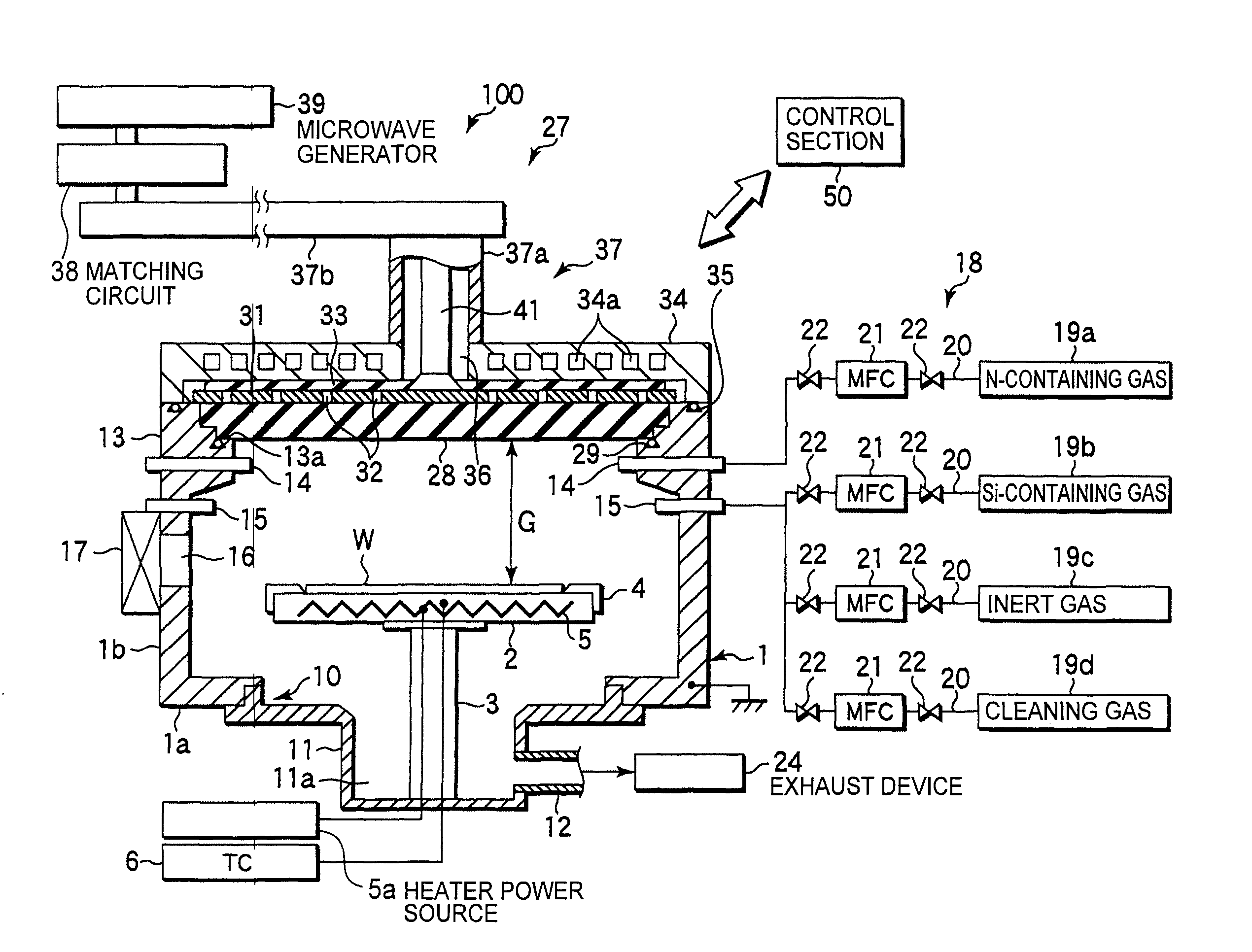
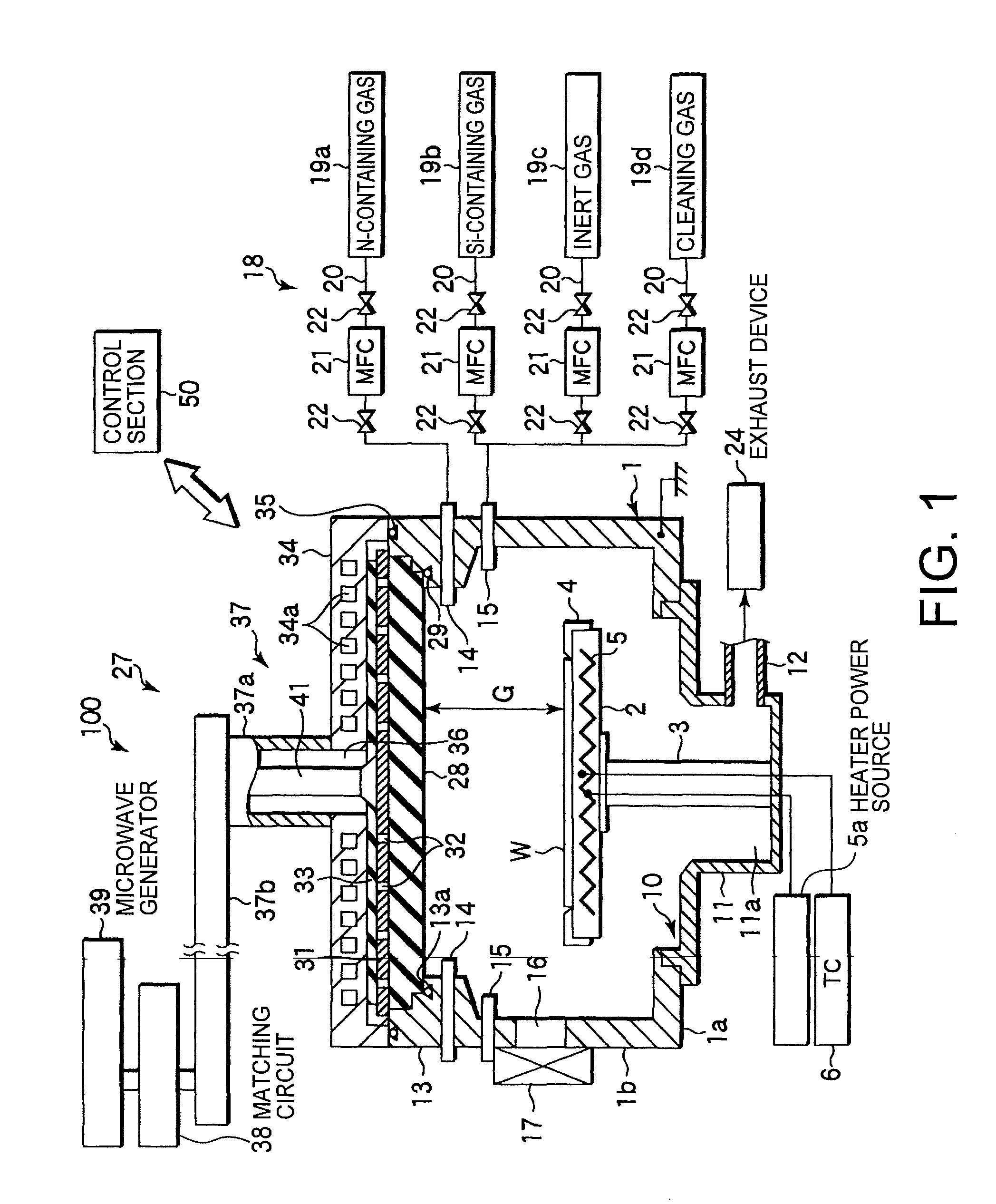
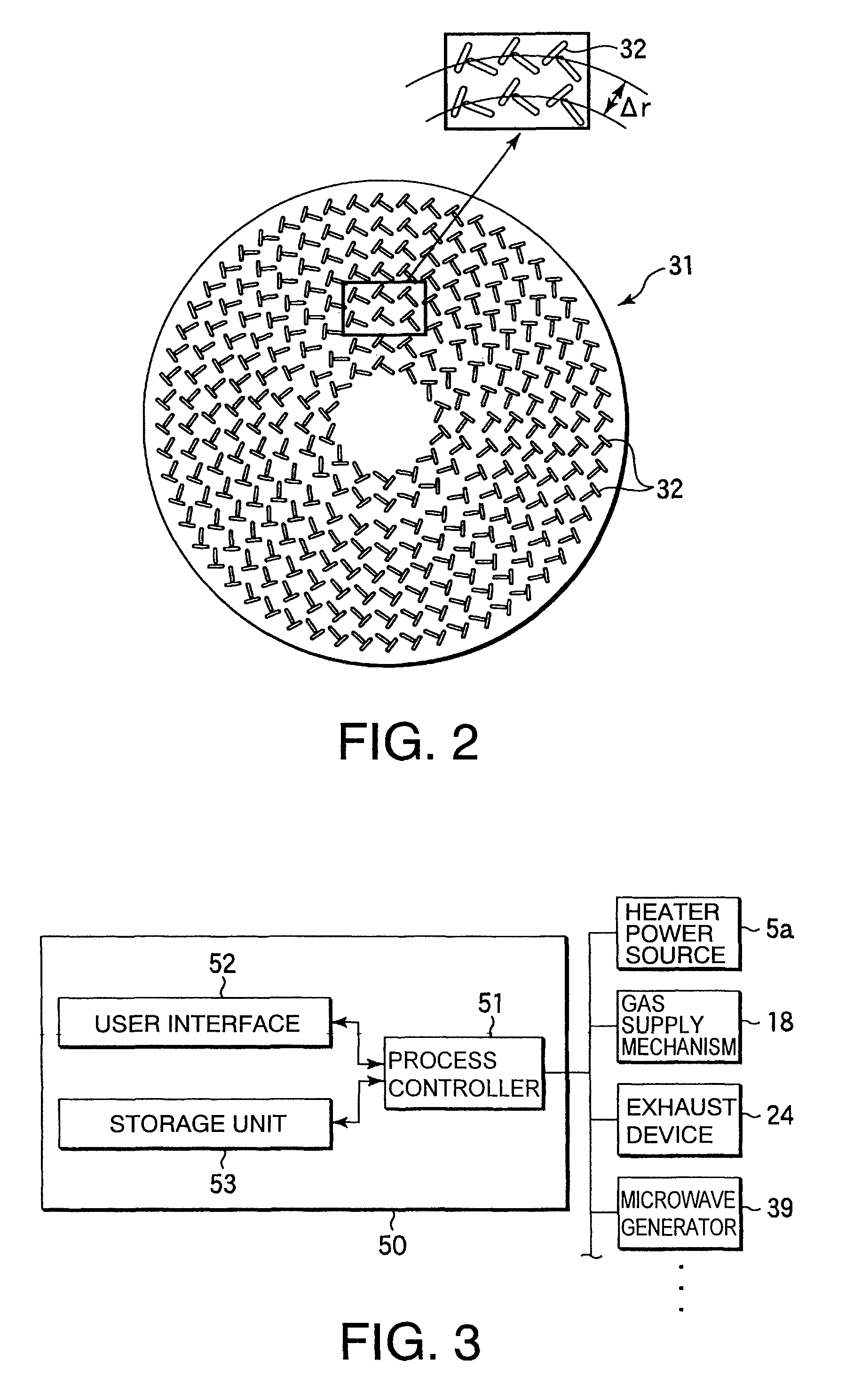
[0044]FIG. 1 is a cross-sectional diagram schematically illustrating the construction of an example of a plasma processing apparatus suited for carrying out a silicon nitride film-forming method according to the present invention; FIG. 2 is a plan view of the plane antenna of the plasma processing apparatus of FIG. 1; and FIG. 3 is a block diagram illustrating the construction of the control section of the plasma processing apparatus of FIG. 1.

[0045]The plasma processing apparatus 100 is constructed as an RLSA microwave plasma processing apparatus capable of generating a high-density, low-electron temperature, microwave-excited plasma by introducing microwaves into a processing chamber by means of an RLSA (radial line slot antenna), which is a plane antenna having a plurality of slot-like holes. The plasma processing apparatus 100 can perform processing with a plasma having a plasma density of 1×10¹⁰ to 5×10¹² / cm3 and a low electron temperature of 0.7 to 2 eV. The ...


PUM

PropertyMeasurementUnit
temperatureaaaaaaaaaa
pressureaaaaaaaaaa
thicknessaaaaaaaaaa

Abstract

A Plasma processing apparatus (100) introduces microwaves into a chamber (1) by a plane antenna (31) which has a plurality of holes. A material gas, which contains a nitrogen-containing compound and a silicon-containing compound, is introduced into the chamber (1) by using the plasma processing apparatus, and plasma is generated by the microwaves. Then, a silicon nitride film is deposited by the plasma on a surface of an object to be processed. The trap density of the silicon nitride film is controlled by adjusting the conditions of the plasma CVD process.

Description

TECHNICAL FIELD[0001]The present invention relates to a method for forming, by plasma CVD (chemical vapor deposition), a silicon nitride film which is useful as a charge storage layer of a nonvolatile semiconductor memory device, and also relates to a method for manufacturing a nonvolatile semiconductor memory device and to a nonvolatile semiconductor memory device, both using the silicon nitride-film forming method.BACKGROUND ART[0002]Current nonvolatile semiconductor memory devices, as typified by electrically rewritable EEPROM (electrically erasable and programmable ROM), include those having a laminate structure, called SONOS (silicon-oxide-nitride-oxide-silicon) type or MONOS (metal-oxide-nitride-oxide-silicon) type. In these types of nonvolatile semiconductor memory devices, holding of information is performed with a silicon nitride film (nitride), sandwiched between silicon dioxide films (oxide), as a charge storage layer. In particular, in such a nonvolatile semiconductor me...

Claims


Application Information

Patent Timeline
Patent Type & Authority Patents(United States)
IPC IPC(8): H01L21/26
CPCC23C16/345C23C16/511H01L21/28282H01L21/3185H01L29/792H01L29/40117H01L21/02274H01L21/02211H01L21/0217H01L21/02107H01L21/28202
Inventor KOHNO, MASAYUKINISHITA, TATSUONAKANISHI, TOSHIOHIROTA, YOSHIHIRO
Owner TOKYO ELECTRON LTD
Why Eureka
Try Eureka