Methods of forming thin films for molecular based devices

a molecular-based device and thin film technology, applied in thermoelectric devices, solid-state devices, instruments, etc., can solve the problems of unsustainable demand for smaller, smarter devices, devices that continue to push the limits of processes and manufacturing equipment, and the size of conventional semiconductor memory cells continues to decreas

Inactive Publication Date: 2012-11-27
ZETTACORE
View PDF35 Cites 8 Cited by
  • Summary
  • Abstract
  • Description
  • Claims
  • Application Information

AI Technical Summary

Benefits of technology

[0013]In another embodiment, a molecular based device is provided, characterized in that a wetting layer is disposed between a substrate and a molecular layer, the wetting layer comprised of a material that promotes equalization of surface tension across the substrate.

Problems solved by technology

There is an un-exhaustive demand for smaller, smarter devices that continue to offer more memory and functionality.
Production of such memory devices continues to push the limits of processes and manufacturing equipment.
Unfortunately, conventional memory, such as silicon-based DRAM memory, has reached a point where continued reduction in the size of conventional semiconductor memory cells is expected to adversely affect at least some of these important parameters.
However, molecular device processing is sensitive to many variables and conditions that are not problems in traditional semiconductor processing.
Additionally, when devices are manufactured with molecular-scale features, problems are magnified and defects at the molecular scale become significant.
Dissimilar surface tensions at these interfaces negatively impact the nucleation behavior of the molecules and the wetting behavior of a subsequently deposited charge transfer layer.
This negatively impacts the ability to scale such structures.
Further, such dissimilar nucleation and wetting behavior results in non-uniformities which degrade signal strength and speed performance, as well as negatively impact the reliability and reproducibility of the device.

Method used


Image

  • Methods of forming thin films for molecular based devices
  • Methods of forming thin films for molecular based devices
  • Methods of forming thin films for molecular based devices

Examples


example 1

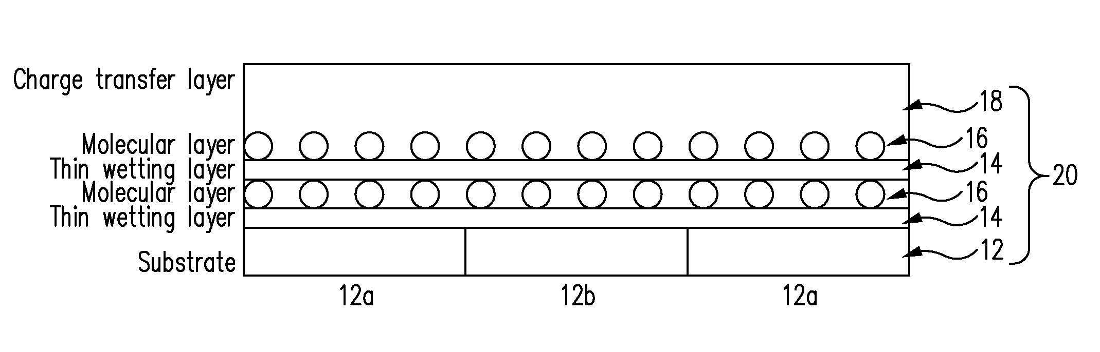
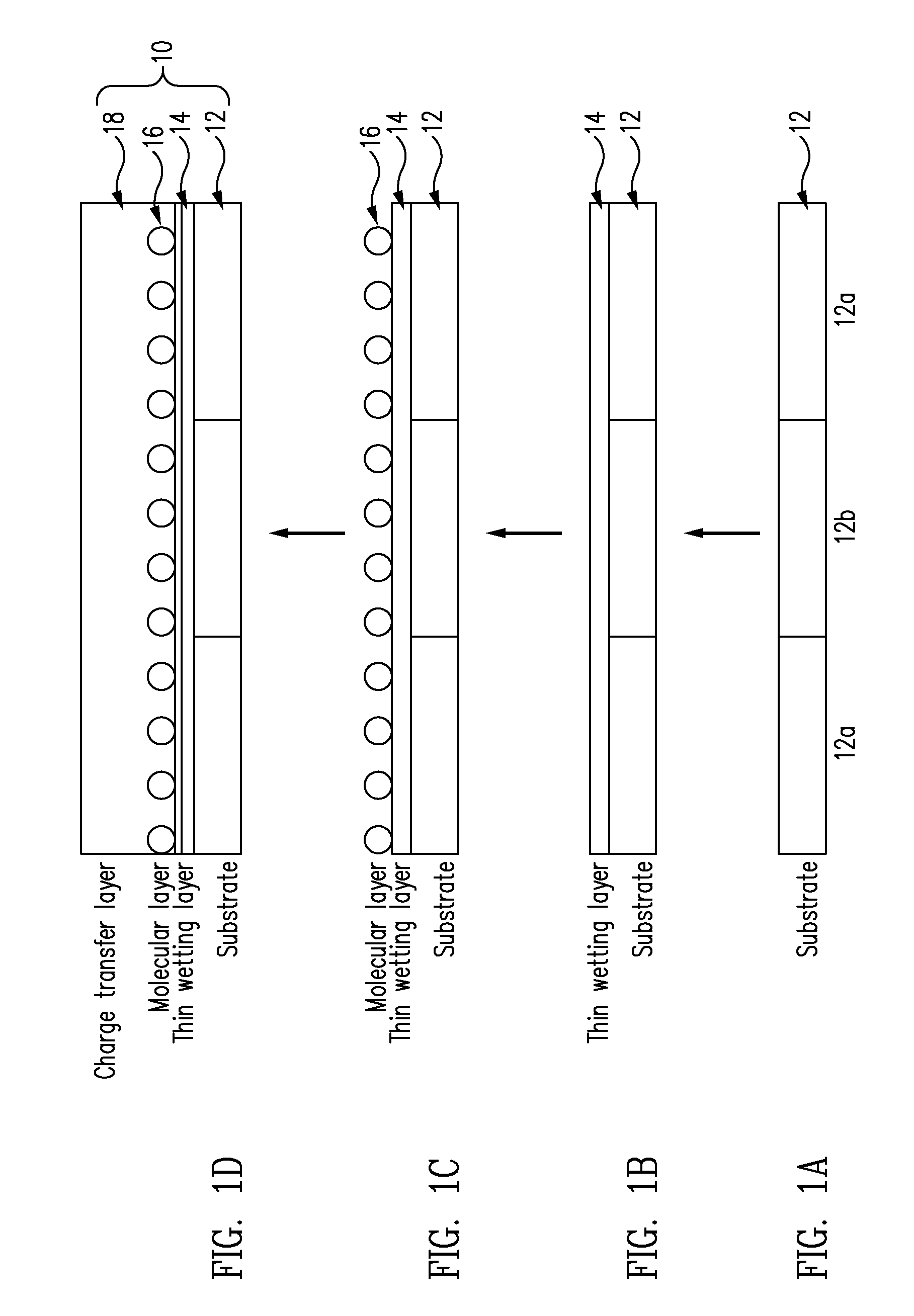
[0178]In general, molecular based devices were formed as described above, and utilizing a wetting layer comprised of TiO2. In this example the wetting layer of TiO2 was formed atop of the molecular layer. In the exemplary embodiment, the TiO2 layer was formed after deposition of the redox-active molecular layer. H2O vapor is flowed in an inert carrier gas at a flowrate in the range of 1 to 50 sccm, for a period of time in the range of 1×10⁻⁵ to 10 seconds. This first step is carried out at a process pressure in the range of 1×10⁻⁵ to 1 Torr. The H2O vapor is then purged from the deposition chamber. Next, tetrakis(dimethylamido) Ti(IV) is flowed into the deposition chamber in an inert carrier gas at a flowrate in the range of 1 to 50 sccm, for a period of time in the range of 1×10⁻⁵ to 10 seconds. This second step is carried out at a process pressure in the range of 1×10⁻⁵ to 1 Torr. The deposition chamber is then purged. FIGS. 4A and 4B depict current and potential curves illustrati...

example 2

[0179]In this example, molecular based devices were formed with a wetting layer comprised of TiO2 deposited below the molecular layer. In the exemplary embodiment, the TiO2 layer was formed after deposition of the redox-active molecular layer. H2O vapor is flowed in an inert carrier gas at a flowrate in the range of 1 to 50 sccm, for a period of time in the range of 1×10⁻⁵ to 10 seconds. This first step is carried out at a process pressure in the range of 1×10⁻⁵ to 1 Torr. The H2O vapor is then purged from the deposition chamber. Next, tetrakis(dimethylamido) Ti(IV) is flowed into the deposition chamber in an inert carrier gas at a flowrate in the range of 1 to 50 sccm, for a period of time in the range of 1×10⁻⁵ to 10 seconds. This second step is carried out at a process pressure in the range of 1×10⁻⁵ to 1 Torr. The deposition chamber is then purged. Following the deposition of the TiO2 wetting layer, the redox-active molecular layer was deposited. FIGS. 5A and 5B depict current a...

example 3

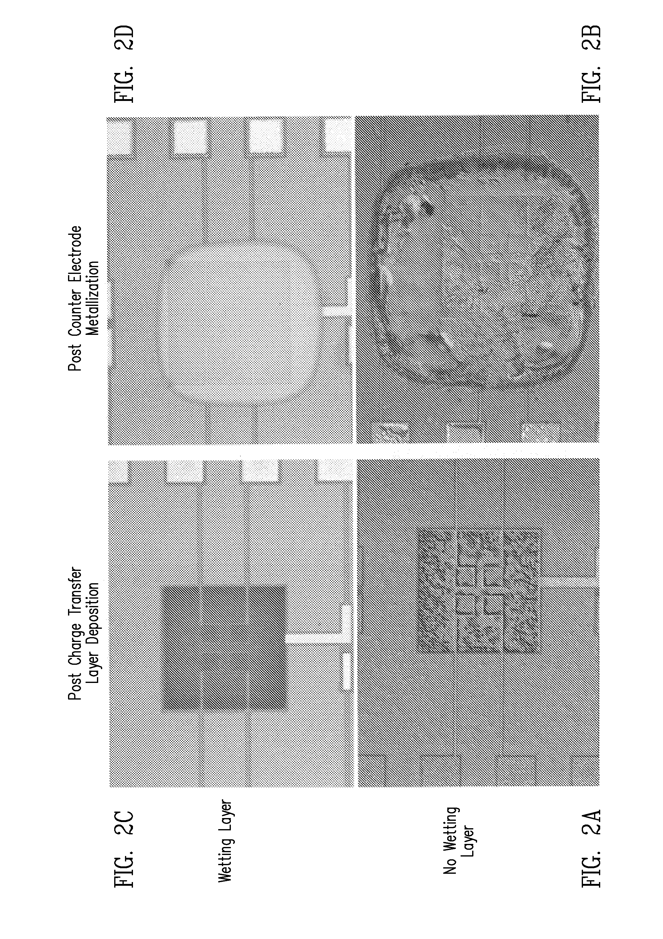
[0180]Impedance ration verses frequency of devices formed according to the present invention were tested as shown in FIGS. 6A and 6B. Three devices were formed by first: depositing 2 cycles of TiO2 layers followed by 20 cycles of TiO2+ redox active molecular layer, using the same process conditions as reported above in Examples 1 and 2. Next, the process was carried out depositing 5 cycles of TiO2 followed by 20 cycles of the redox active molecular layer, and finally 20 cycles of the redox active molecular layer without any TiO2 layer. The speed at which the redox-active molecular layer performs was judged by measuring the impedance of the device at 1) a potential where no redox activity from the molecular layer occurs (Off Peak) and 2) at potential where the redox-active layer is oxidized and reduced (Peak). The ratio of the impedance at these two potentials is indicative of the amount of charge from the redox-active layer (magnitude of the y-axis) and the maximum speed the molecul...


PUM


Abstract

The invention generally encompasses methods of forming thin films molecular based devices, and devices formed therefrom. Some embodiments relate to molecular memory cells, molecular memory arrays, electronic devices including molecular memory, and processing systems and methods for producing molecular memories. More particularly, the present invention encompasses methods and molecular based devices comprising a wetting layer and redox-active molecules.

Description

CROSS REFERENCE TO RELATED APPLICATIONS[0001]This application claims the benefit of, and priority to, U.S. Provisional Patent Application Ser. No. 61 / 102,305 filed on Oct. 2, 2008, entitled “Methods of Forming Thin Films for Molecular Based Devices,” the entire disclosure of which is incorporated herein by reference.FIELD OF THE INVENTION[0002]The invention broadly encompasses methods of forming thin films for molecular based devices, and devices formed therefrom. Some embodiments relate to molecular memory cells, molecular memory arrays, electronic devices including molecular memory, and processing systems and methods for producing molecular memories. More particularly, in some embodiments the present invention encompasses methods and molecular based devices comprising a wetting layer formed between a substrate and an active molecular layer.BACKGROUND OF THE INVENTION[0003]As device densities decrease, new developments in the design of semiconductor and other electronic devices rec...

Claims


Application Information

Patent Timeline
Patent Type & Authority Patents(United States)
IPC IPC(8): H01L35/24
CPCH01L51/0591H01L51/0595G11C13/0014H10K10/50H10K10/701
Inventor SORENSON, THOMAS A.EASTEP, BRIANGAHERTY, LEESNOW, TIMOTHY L.
Owner ZETTACORE
Why Eureka
Try Eureka