Electron microscope with integrated detector(s)

a detector and electron microscope technology, applied in material analysis using wave/particle radiation, instruments, nuclear engineering, etc., can solve the problems of reducing affecting the optical performance of the microscope, and the tube diameter increase limits the optimal placement of the detector, etc., to achieve the effect of efficient and economical manner

Active Publication Date: 2012-12-18
FEI CO
View PDF35 Cites 12 Cited by
  • Summary
  • Abstract
  • Description
  • Claims
  • Application Information

AI Technical Summary

Benefits of technology

[0051]1. It permits more optimal placement of the sensor(s) relative to the specimen since the sensor need not be located at the end of a straight rod or tube inserted from a mounting surface exterior to the microscope.
[0066]A third aspect of the present invention is that it teaches a particularly efficient and economical manner of accommodating multiple sensors, resulting in novel configurations of sensors that have not heretofore been practiced as a single detector system.

Problems solved by technology

For the Si(Li) detector, this strategy is limited by the direct relationship between detector noise and active area, meaning that resolution rapidly degrades as detector size increases.
Though such increases in detector size are certainly beneficial in certain respects, they also have drawbacks, and especially within the context of the conventional tubular-mount EDX design.
The diameter of the detector tube must accommodate the size of the sensor device with allowance for mounting and connections, and this increased tube diameter limits the optimal placement of the detector.
To avoid these consequences, it would be necessary to increase the working distance of the specimen to the face of the final focusing lens, which is in turn detrimental to the optical performance of the microscope.
In addition to such geometrical considerations, increasing the detection efficiency by increasing detector area creates other problems when there is a large flux of x-rays impinging on the detector.
However, at such high rates there is also an increased probability of “summing events” in which two different x-ray emissions reach the detector so close together in time that they cannot be distinguished as separate events.
This effect leads to “sum peaks” and other artifacts in the measured x-ray spectrum, and this in turn creates problems relative to accurate analysis.
Thus, a large-area detector operated in close proximity to a specimen may be advantageous for analytical circumstances where the x-ray rate is low, but is problematic when the rate is high.
However, exercising either of these strategies tends to defeat the point of a large-area detector, and neither of these strategies is optimal when the specimen has both high-emission and low-emission regions.
Finally, there are other, more subtle issues associated with very-large-area x-ray sensors.
One is that the large sensitive area makes it more difficult to collimate the x-ray path to accept x-rays emitted from the point of beam impact and exclude those produced by scattered electrons striking elsewhere.
Also, although the energy resolution of SDD detectors does not degrade as significantly as for the Si(Li) detector as the sensor area is increased, there is still some loss of resolution in the current generations of SDD devices.
And finally, large-area SDD sensors of spectroscopic quality are substantially more expensive at present than smaller devices.
Thus, the strategy of increasing x-ray detection efficiency by increasing the area of the sensor element is a viable option up to a point, and then other factors increasingly diminish its attractiveness.
This has sometimes been employed with Si(Li) detectors for specialized applications where x-ray collection speed is very important, the microscope is equipped with appropriate mounting ports, and the high cost is warranted.
There is also growing recognition that multiple detectors can not only provide greater sensitivity, but can facilitate the analysis of non-flat specimens (such as particulate specimens or fracture surfaces) where topographic effects (such as shadowing) can produce misleading results via a single detector.
However, because of the intrinsic size of such an array, this kind of detector requires an especially large mounting tube and thus again sacrifices some sensitivity due to setback from the specimen.
However, this sensor occupies the position normally reserved for a BSE detector, and it is thus not suitable for the many applications where a high-quality BSE signal is required.
Such detectors combine certain of the advantages of both the large area detector and multiple detectors, but they are presently rather costly devices whose special interfacing requirements present challenges for installation in some microscopes.
Consequently, beryllium window (BeW) detectors are not generally useful for measuring elements lower than fluorine in the periodic table.
However, UTW detectors require a magnetic electron trap to prevent energetic scattered electrons from penetrating the x-ray window and striking the sensor, thus corrupting the measured x-ray spectrum.
Because the strength of the permanent magnets employed in such a trap is limited by available magnet technology, an increase in the aperture area of such a trap necessarily results in weakened deflection field strength while the amount of required deflection is simultaneously increased.
This consideration is applicable for both single element sensors and multi-element sensor arrays and can represent a significant limitation to attainable solid angle when light-element detection is required.
The tilted-sensor detector was encountered rather commonly in the early days of EDX technology because electron microscopes of the day had not been designed for installation of high-takeoff-angle detectors.
This strategy works reasonably well for small-area detectors, but becomes cumbersome to implement as the sensor size is increased.
It has thus far had limited use for an SDD type of detector.
The relative unpopularity of this type of mount can be largely attributed to the difficulty in installing a large-area sensor or sensor module in a non-axial orientation within the conventional tube-type mount.

Method used


Image

  • Electron microscope with integrated detector(s)
  • Electron microscope with integrated detector(s)
  • Electron microscope with integrated detector(s)

Examples


example 1

Basic Single-Sensor Detector

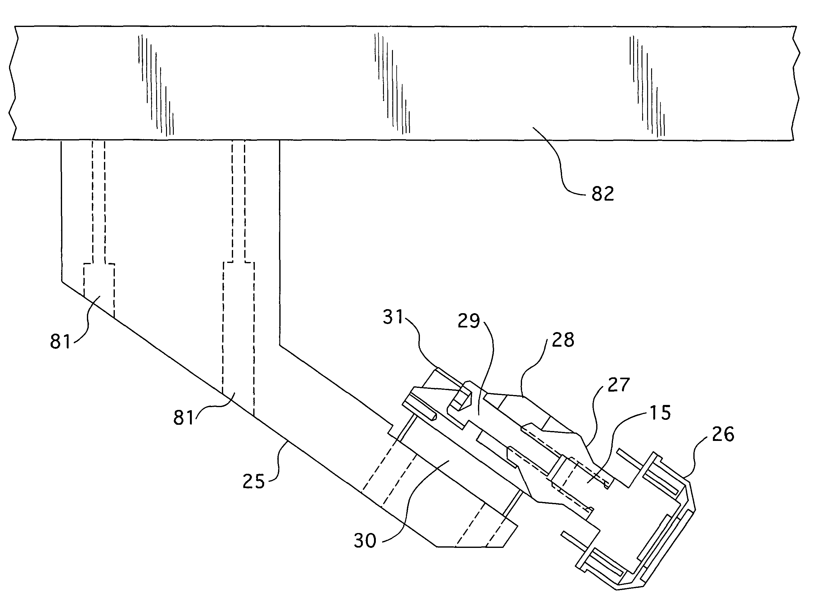
[0079]FIG. 5 illustrates a very basic implementation of an integrated EDX detector constructed with a packaged SDD module. The mounting bracket [25] is designed to be attached to the flat “ceiling” surface of the specimen chamber [82] of a particular SEM by means of screw passage holes [81] provided. The detector element [26] is a packaged SDD module [20] of the type shown in FIG. 3. The dimensions of the mounting bracket [25] are chosen such that the SDD module [26] is held in the desired proximity to the specimen with its axis pointing at the nominal impingement point of the microscope's electron beam on the specimen. The threaded thermal stud [15] of the packaged SDD module [26] is screwed tightly into a tapped hole located in the front of the thermal interface stub [27] whose rear portion is tapered and provided with a central tapped hole. The role of the thermal interface stub is to provide an efficient thermal bridge between the packaged SDD module ...

example 2

A Column-Integrated Array Detector

[0089]The prior example illustrated the practical benefits that can be achieved with a very simple application of certain of the principles herein taught. This second example illustrates a more sophisticated implementation that incorporates additional novel practices and provides additional benefits.

[0090]It will have become apparent that an important key to accomplishing an efficient integration of a packaged SDD module into an electron microscope is in achieving a compact thermally-efficient coupling of the packaged SDD module to the secondary TEC module. FIG. 6 illustrates such a mounting. Here the thermal stud of the packaged SDD module [26] is screwed into a tapped hole in the stem of a “tee-shaped” copper stub [32] whose flat face is in contact with the cold face of the second TEC module [30]. A clamping plate [33] with a central opening is employed to clamp the warm face of the second TEC module [30] against a flat thermally-dissipative surfa...


PUM

PropertyMeasurementUnit
areasaaaaaaaaaa
areaaaaaaaaaaa
areaaaaaaaaaaa

Abstract

An electron microscope including a vacuum chamber for containing a specimen to be analyzed, an optics column, including an electron source and a final probe forming lens, for focusing electrons emitted from the electron source, a specimen stage positioned in the vacuum chamber under the probe forming lens for holding the specimen, and an x-ray detector positioned within the vacuum chamber. The x-ray detector includes an x-ray sensitive solid-state sensor and a mechanical support system for supporting and positioning the detector, including the sensor, within the vacuum chamber. The entirety of the mechanical support system is contained within the vacuum chamber. Multiple detectors of different types may be supported within the vacuum chamber on the mechanical support system. The mechanical support system may also include at least one thermoelectric cooler element for thermo-electrically cooling the x-ray sensors.

Description

CROSS REFERENCE[0001]This application depends upon U.S. Provisional Application No. 61 / 216,290, filed 15 May 2009, entitled ELECTRON MICROSCOPE WITH INTEGRATED DETECTOR(S), the entirety of which is incorporated herein by reference.BACKGROUND OF THE INVENTION[0002]The invention pertains to the integration of semiconductor x-ray radiation sensors within a Scanning Electron Microscope (SEM) or similar analytical electron-beam instrument, optionally in conjunction with a backscattered electron sensor. The invention pertains to novel methods of configuring both the detection elements and the microscope so as to achieve improvements in performance and economies of construction, as well as other benefits.[0003]The installation of a solid-state Energy Dispersive X-ray (EDX) detector onto an electron microscope was first reported by Fitzgerald, Keil, and Heinrich in 1968. The type of detector described was a lithium-drifted silicon (Si(Li)) diode that was introduced through the port of an el...

Claims


Application Information

Patent Timeline
Patent Type & Authority Patents(United States)
IPC IPC(8): G01N23/00
CPCH01J37/244H01J37/256H01J37/28H01J2237/2807H01J2237/24415
Inventor SCHAMBER, FREDERICK H.VAN BEEK, CORNELIS G.
Owner FEI CO
Why Eureka
Try Eureka