Charged particle beam applied apparatus

a technology of charged particles and applied apparatuses, which is applied in the direction of material analysis using wave/particle radiation, semiconductor/solid-state device testing/measurement, instruments, etc., can solve the problems of long time, improvement of specimen processing speed, and difficulty in shortening the distance between the positions illuminated by the electron source, so as to achieve the effect of convenient implementation

Active Publication Date: 2013-01-08
HITACHI HIGH-TECH CORP
View PDF17 Cites 67 Cited by
  • Summary
  • Abstract
  • Description
  • Claims
  • Application Information

AI Technical Summary

Benefits of technology

[0017]The present invention realizes an easily-implementable charged particle beam applied apparatus that can apply charge-control beams and signal-detection beams under a number of separate conditions.

Problems solved by technology

Many of these charged particle beam applied apparatuses employ a technique of scanning a focused charged particle beam on a specimen; however, this technique requires a long time for inspecting the entire surface of the specimen, and therefore improvement of the specimen processing speed is an important issue.
In addition to the improvement of the specimen processing speed, these charged particle beam applied apparatuses are required, as an important issue, to improve the accuracy of defect detection and measurement in accordance with the increase in miniaturization and complexity of devices.
However, an electron optical column provided with the electron source of signal-detection beams and an electron optical column provided with the pre-charge electron source have specified dimensions, respectively, that make it difficult to shorten the distance between the positions illuminated by the electron sources.
Owing to the time difference, some specimens may not be able to maintain their charge provided by the pre-charge beam until the signal-detection beam illuminates the specimens.

Method used


Image

  • Charged particle beam applied apparatus
  • Charged particle beam applied apparatus
  • Charged particle beam applied apparatus

Examples


embodiment 1

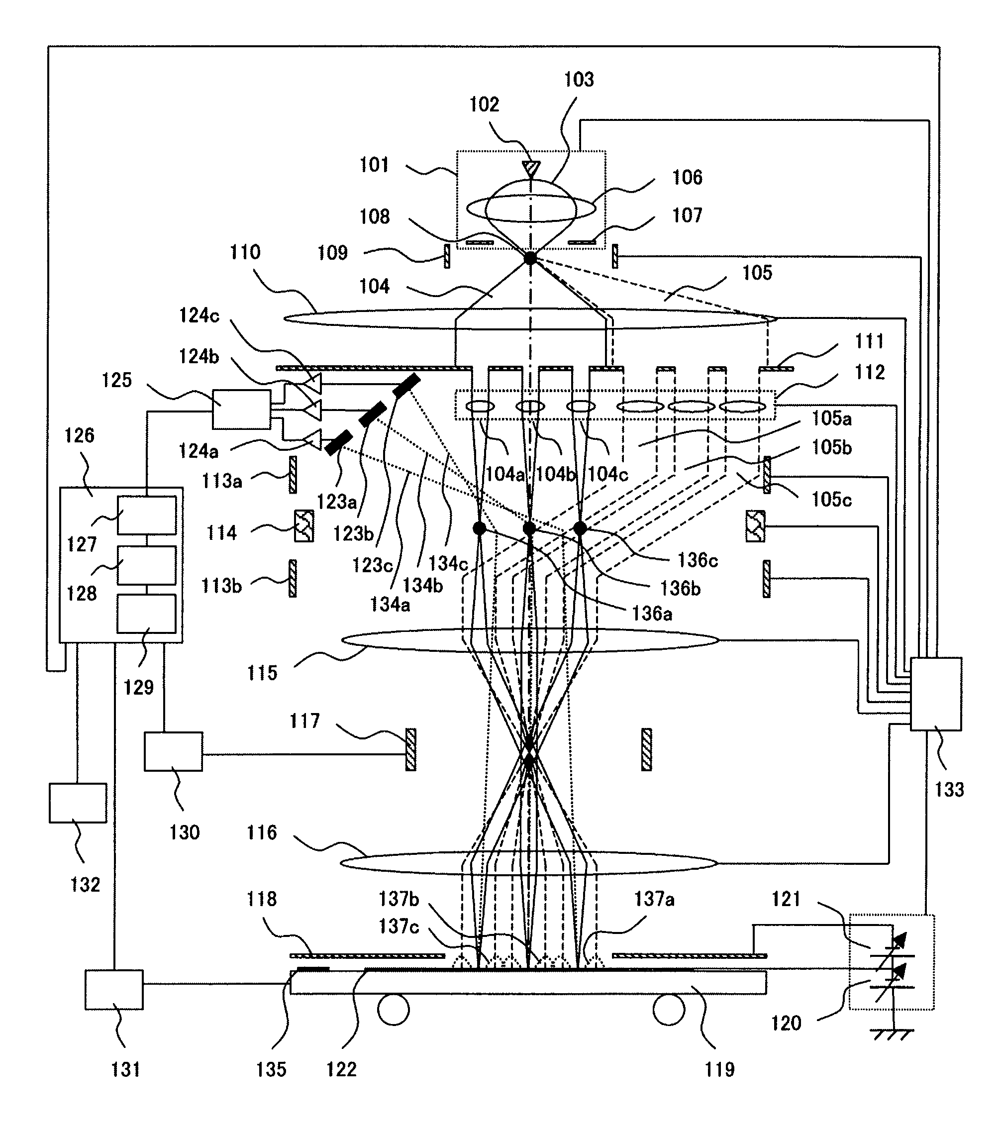
[0038]Described in the first embodiment is a multi-beam type scanning electron microscope including an aperture array and a lens array, both having multiple aperture patterns, further including a deflector that is disposed at the position of an electron source image above the aperture array and selects an aperture pattern, and changing the temporal timing between pre-charge and inspection. Thus configured apparatus realizes: with an easily-implementable configuration, change / switch of the timing between charge-control beam illumination and signal-detection beam illumination and reduction of time difference from the charge-control beam illumination to the signal-detection beam illumination to control charge and detect signals under optimal conditions, thereby improving defect detection sensitivity.

[0039]FIG. 1 is a schematic diagram of an electron beam inspection apparatus according to Embodiment 1. First of all, the configuration of the apparatus will be described. An electron gun 1...

embodiment 2

[0085]In Embodiment 1, switching between the illumination conditions of the charge-control beam and the illumination conditions of the signal-detection beam takes place in synchronization with scan signals to reduce the time difference from illumination by charge-control beams to illumination by signal-detection beams, thereby enabling an inspection with a wafer steadily charged. However, the embodiment may sometimes pose nonuniformity in image brightness and inspection sensitivity of every beam. To overcome the problem, the second embodiment provides an inspection method realizing uniform image brightness and inspection sensitivity.

[0086]First of all, the reason why the image brightness and inspection sensitivity of every beam become nonuniform in Embodiment 1 will be described with reference to FIGS. 7A, 7B and FIGS. 8A, 8B. FIG. 8A illustrates time variations of the amount of charge at a charge-control beam illuminated part. The amount of charge increased by a charge-control beam...

embodiment 3

[0090]In Embodiments 1 and 2, the conditions for the charge-control beams 702a to 702e and the conditions for the signal-detection beams 703a to 703e are switched over every time the beams sweep from one boundary to the other boundary of the beam illumination regions 701a to 701e; however, every switching operation of the illumination conditions takes a few seconds. The methods of Embodiments 1 and 2 that involve frequent switching of the illumination conditions may sometimes cause a long inspection time. If, however, the wafer 122 can hold the charge roughly equal to or longer than the time required to scan a stripe, it is enough to switch the conditions between charge-control beam illumination and signal-detection beam illumination every time one stripe is scanned. In the third embodiment, the above-described two conditions are switched every time one stripe is scanned. The third embodiment can reduce the number of times to switch the illumination conditions and reduce the duratio...


PUM

PropertyMeasurementUnit
timeaaaaaaaaaa
surface electric fieldaaaaaaaaaa
surface electric-fieldaaaaaaaaaa

Abstract

Provided is a multi-beam type charged particle beam applied apparatus in an implementable configuration, capable of achieving both high detection accuracy of secondary charged particles and high speed of processing characteristically different specimens. An aperture array (111) includes plural aperture patterns. A deflector (109) for selecting an aperture pattern through which a primary beam passes is disposed at the position of a charged particle source image created between an electron gun (102), i.e., a charged particle source, and the aperture array (111). At the time of charge-control beam illumination and at the time of signal-detection beam illumination, an aperture pattern of the aperture array (111) is selected, and conditions of a lens array (112), surface electric-field control electrode (118) and the like are switched in synchronization with each beam scanning. Thus, the charges are controlled and the signals are detected at different timings under suitable conditions, respectively.

Description

TECHNICAL FIELD[0001]The present invention relates to charged particle beam application technologies, and more particularly to charged particle beam applied apparatuses, such as inspection apparatuses and measurement apparatuses, used in manufacturing processes of semiconductors and magnetic disks.BACKGROUND ART[0002]In a process of manufacturing semiconductors or magnetic disks, use is made of a charged particle beam applied apparatus to perform measurement, defect review, inspection or the like of a specimen through observation that includes illuminating the specimen with a charged particle beam (hereinafter, referred to as a signal-detection beam), such as an electron beam and an ion beam, detecting produced secondary charged particles, such as secondary electrons, and performing arithmetic computations on signals obtained from the detected secondary charged particles.[0003]Many of these charged particle beam applied apparatuses employ a technique of scanning a focused charged pa...

Claims


Application Information

Patent Timeline
Patent Type & Authority Patents(United States)
IPC IPC(8): H01L21/66G01N23/225
CPCB82Y10/00B82Y40/00H01J37/3023H01J37/3177G01R31/305H01J2237/004H01J2237/0044
Inventor OTAKI, HIROKIENYAMA, MOMOYOOHTA, HIROYA
Owner HITACHI HIGH-TECH CORP
Why Eureka
Try Eureka