Recordable optical storage medium comprising a semiconductor layer, and respective manufacturing method
a semiconductor layer and optical storage medium technology, applied in optical recording/reproducing/erasing methods, instruments, photomechanical equipment, etc., can solve the problem of comparatively high laser power needed to activate the mask layer, and achieve the effect of increasing the reflectivity of the indium alloy semiconductor layer, reducing the need for laser power, and low reflectivity
- Summary
- Abstract
- Description
- Claims
- Application Information
AI Technical Summary
Benefits of technology
Problems solved by technology
Method used
Image

Examples
Embodiment Construction
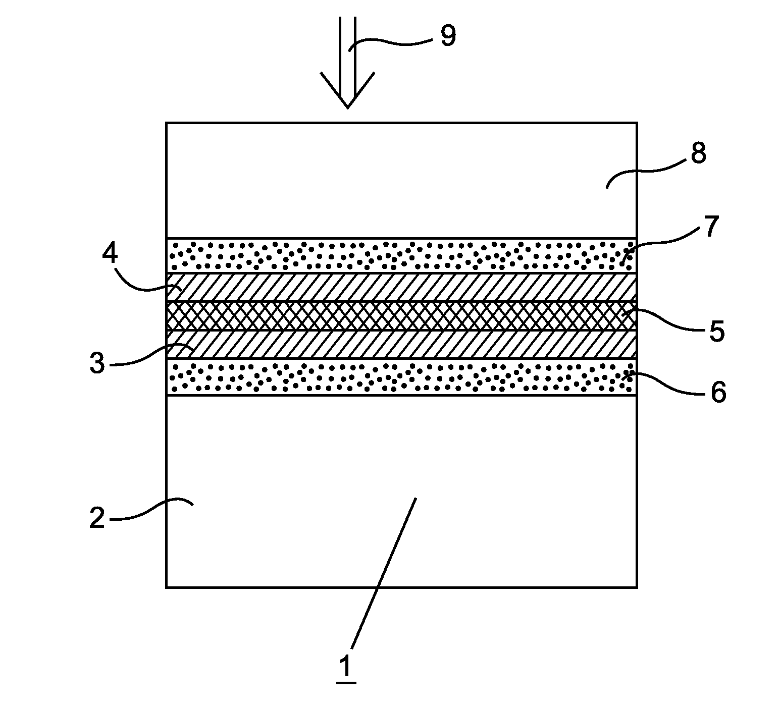
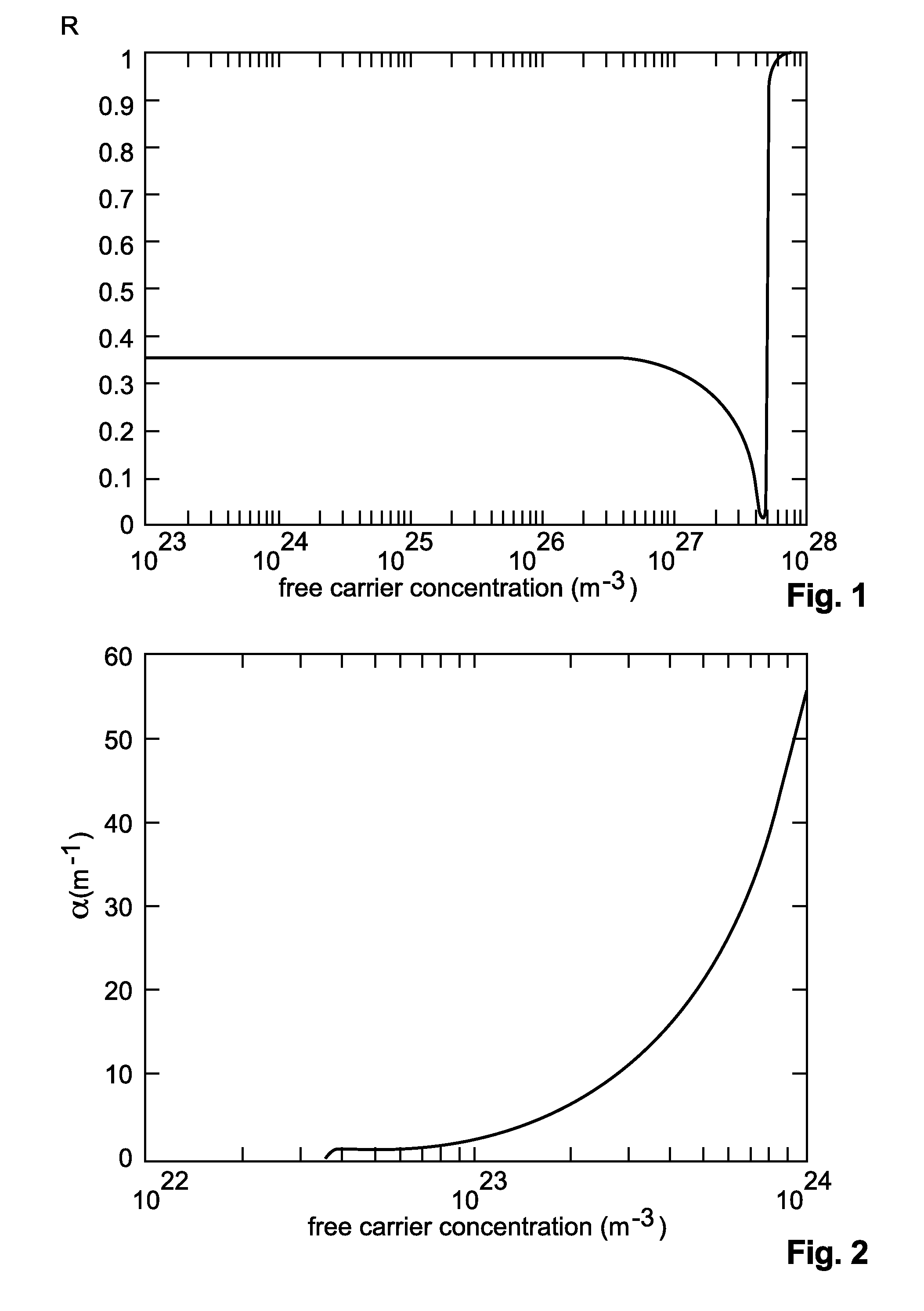
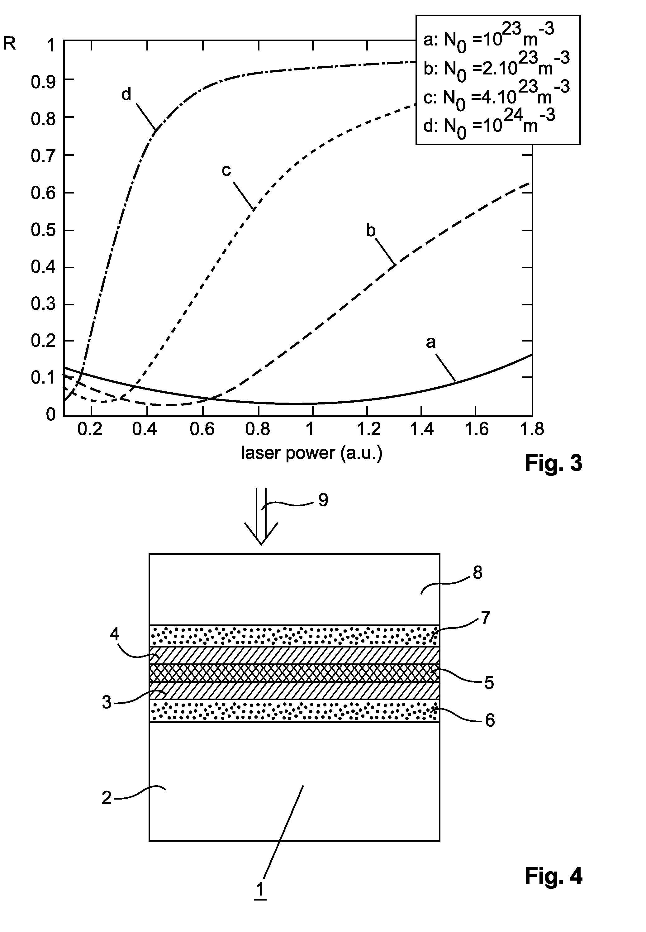
[0022]The reflectivity R of a thin semiconductor layer is a function of the free carrier concentration and the thickness of the layer. The free carrier concentration can be calculated by using the Drude model of free electrons in solids. For a semiconducting layer with a thickness d, one can write the free carrier concentration N as follows:
[0023]N∝(1-R)·[1-exp(-αd)]1d
where α is the absorption coefficient of the material. The resulting reflectivity R as a function of the free carrier concentration is shown in FIG. 1 for an InSb layer. As can be seen, above a certain threshold of the free carrier concentration, the reflectivity rises to a level of almost one.
[0024]The dependency between the absorption coefficient α and the free carrier concentration N is shown in FIG. 2, which shows the calculated absorption coefficient α as a function of the free carrier concentration for an InSb layer. Thus, by increasing α, the free carrier concentration will be enhanced.
[0025]If the semicondu...
PUM
| Property | Measurement | Unit |
|---|---|---|
| laser wavelength | aaaaa | aaaaa |
| length | aaaaa | aaaaa |
| length | aaaaa | aaaaa |
Abstract
Description
Claims
Application Information