

Hole blocking layers in non-polar and semi-polar green light emitting devices
a technology of green light emitting device and hole blocking layer, which is applied in the direction of lasers, semiconductor lasers, solid-state devices, etc., can solve the problem of difficult to limit the formation of misfit dislocations
- Summary
- Abstract
- Description
- Claims
- Application Information
AI Technical Summary
Benefits of technology
Problems solved by technology
Method used
Image

Examples
Embodiment Construction
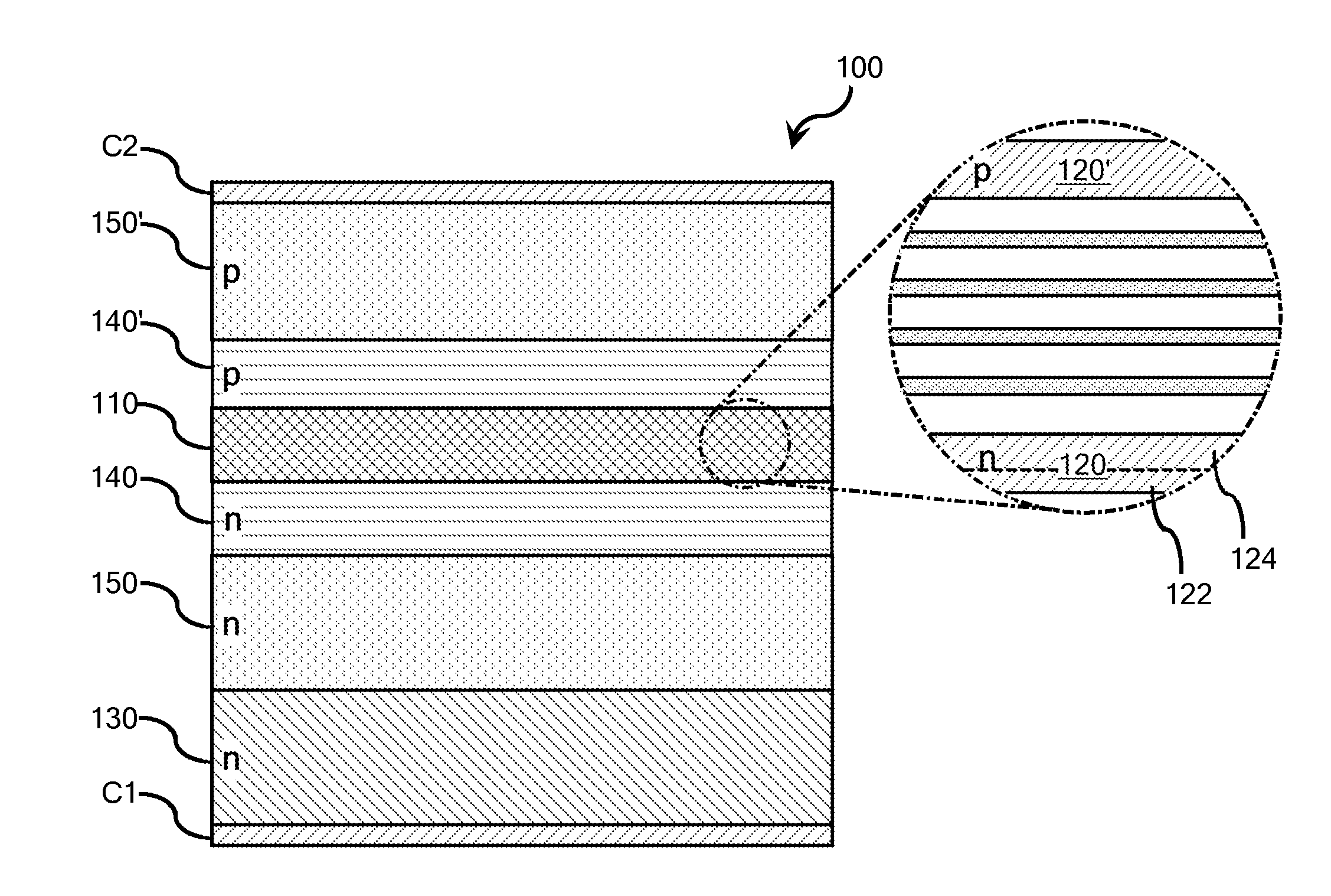
[0007]The concepts of the present disclosure can be illustrated in the context of two different types of semiconductor-based light emitting devices—a laser diode 100 (FIG. 1) and a light emitting diode 200 (FIG. 2). The laser diode 100 illustrated in FIG. 1 comprises an active region 110 interposed between n-type and p-type sides of the device and a hole blocking layer (HBL) 120 interposed between the active region 110 and the n-type side of the device. The n-type and p-type sides of the laser diode 100 generally comprise n-doped and p-doped semiconductor regions, described in further detail below, and device contact layers C1, C2.
[0008]The active region 110 of the laser diode 100 comprises an active MQW structure and is configured for electrically-pumped stimulated emission of photons in the green portion of the optical spectrum. The n-type side of the laser diode 100 comprises an n-doped semiconductor region composed of an n-doped non-polar or n-doped semi-polar substrate 130, an ...
PUM
 Abstract
Description
Claims
Application Information