Metal etch stop fabrication method and structure

a technology of metal etching and fabrication method, applied in the field of substrates, can solve the problem of reliably plated relative large circuit pattern artifacts

Active Publication Date: 2013-02-26
AMKOR TECH SINGAPORE HLDG PTE LTD
View PDF82 Cites 8 Cited by
  • Summary
  • Abstract
  • Description
  • Claims
  • Application Information

AI Technical Summary

Benefits of technology

[0010]By using the first carrier as the electroplating electrode for plating of the first patterned etch stop layer and the first patterned conductor layer, an electroless plating operation and associated desmear process are avoided. This simplifies manufacturing and reducing fabrication cost as compared to using an electroless plating operation.
[0011]Further, by using the first carrier as the electroplating electrode, relatively large circuit pattern artifacts are reliably plated.
[0012]In one embodiment, an automatic optical inspection (AOI) is performed to inspect the substrate and the various features formed therein for defects. The automatic optical inspection is performed on a single layer, allowing rework of the substrate to correct any defects found. Further, in the event that the defect requires scrapping of the substrate, the substrate is a relatively low cost single layer substrate compared to a multilayer substrate. In either event, performing the automatic optical inspection on a single layer maximizes yield and minimizes fabrication cost.
[0014]The first carrier and second carrier are removed using a carrier etch process. As the etch stop metal of the first and second patterned etch stop layers is selectively etchable compared to a conductor metal of the first and second patterned conductor layers as well as the first and second carriers, the first and second patterned etch stop layers provide an etch stop for the carrier etch process. In this manner, etching of the first and second patterned conductor layers during the carrier etch process is avoided.
[0016]The first patterned etch stop layer and the second patterned etch stop layer provide an etch stop for the via conductor layer etch process. In this manner, etching of the first and second patterned conductor layers during the via conductor layer etch process is avoided.
[0017]By preventing the patterned conductor layers from being etched during the removal of the carriers and the removal of the over-plated via conductor layer, the height and width, i.e., cross-sectional area, of the patterned conductor layers is guaranteed thus insuring that impedance is controlled to within tight tolerance.

Problems solved by technology

Further, by using the first carrier as the electroplating electrode, relatively large circuit pattern artifacts are reliably plated.

Method used


Image

  • Metal etch stop fabrication method and structure
  • Metal etch stop fabrication method and structure
  • Metal etch stop fabrication method and structure

Examples


Embodiment Construction

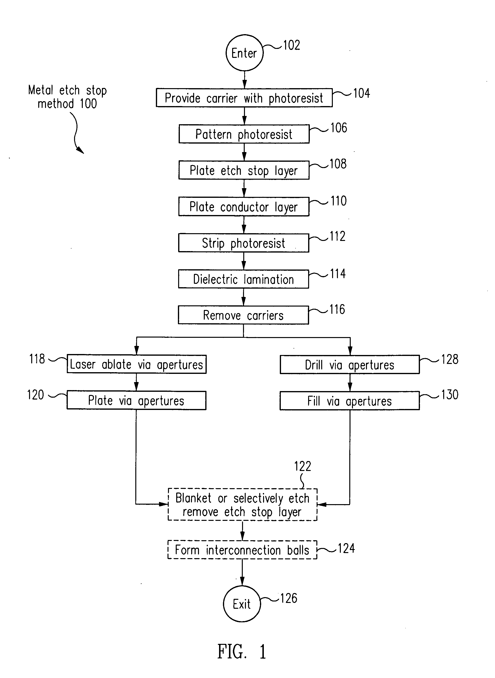
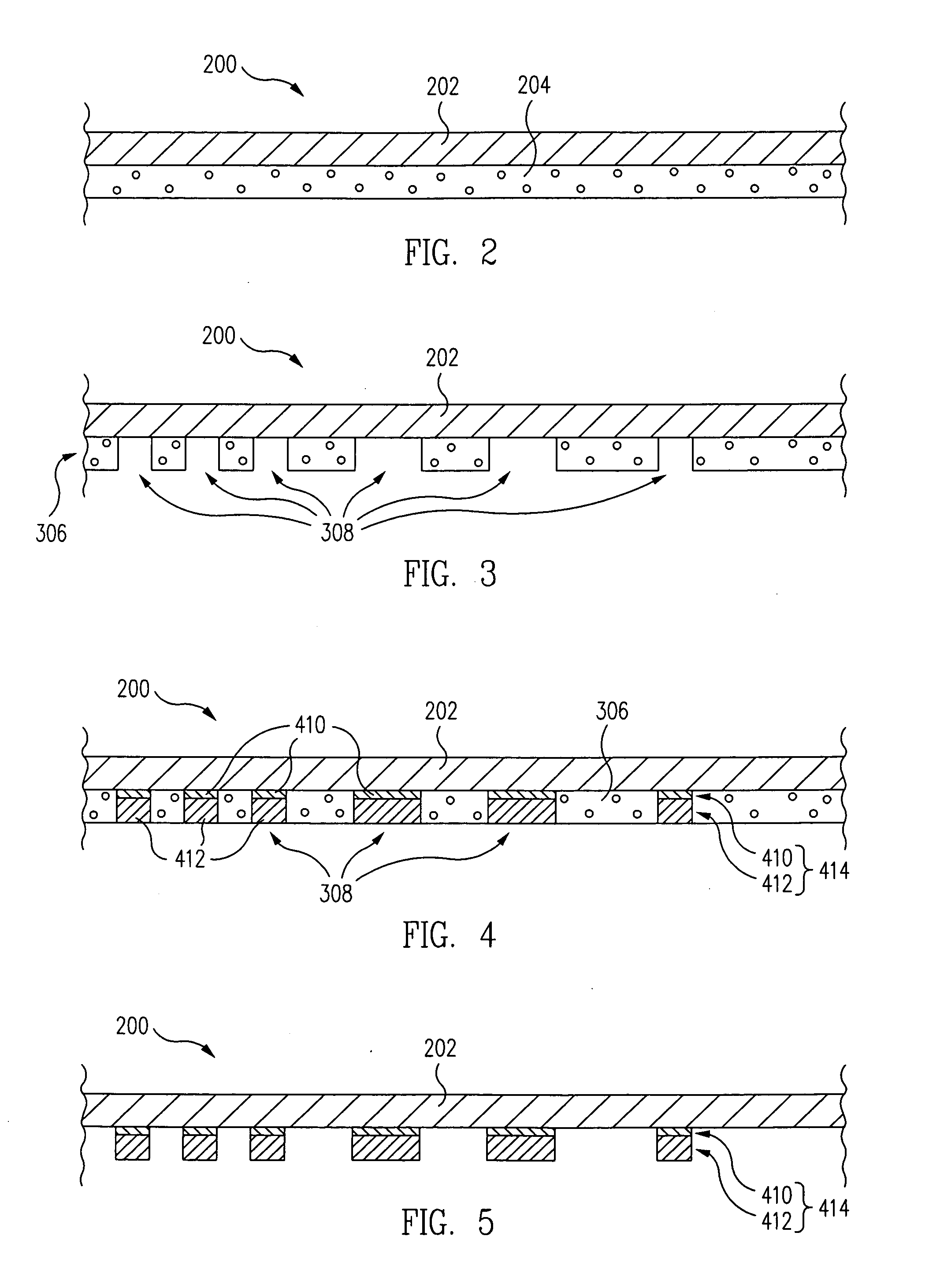
[0034]FIG. 1 is a metal etch stop method 100 for fabricating an electronic component substrate in accordance with one embodiment of the present invention. FIG. 2 is a cross-sectional view of a substrate 200 during fabrication in accordance with one embodiment. FIGS. 3, 4, 5, 6, 7, 8, 9, 10, 11, 12, 13, 14 are cross-sectional views of substrate 200 of FIG. 2 at various stages during fabrication in accordance with various embodiments of the present invention.

[0035]Referring now to FIGS. 1 and 2 together, from an ENTER OPERATION 102, flow moves to a PROVIDE CARRIER WITH PHOTORESIST OPERATION 104. In PROVIDE CARRIER WITH PHOTORESIST OPERATION 104, substrate 200 including a carrier 202 and a photoresist layer 204 is provided.

[0036]Carrier 202 is an electrically conductive material, e.g., copper. Photoresist layer 204 is a layer of photoresist, e.g., positive or negative photoresist, on carrier 202.

[0037]Referring now to FIGS. 1, 2 and 3 together, from PROVIDE CARRIER WITH PHOTORESIST OPE...


PUM

PropertyMeasurementUnit
thickaaaaaaaaaa
electrically conductiveaaaaaaaaaa
conductoraaaaaaaaaa

Abstract

A first patterned etch stop layer and a first patterned conductor layer are laminated by a dielectric material to a second patterned etch stop layer and a second patterned conductor layer. As the etch stop metal of the first and second patterned etch stop layers is selectively etchable compared to a conductor metal of the first and second patterned conductor layers, the first and second patterned etch stop layers provide an etch stop for substrate formation etch processes. In this manner, etching of the first and second patterned conductor layers is avoided insuring that impedance is controlled to within tight tolerance.

Description

RELATED APPLICATIONS[0001]This application is a continuation of Huemoeller et al., U.S. patent application Ser. No. 11 / 765,806, filed on Jun. 20, 2007, entitled “METAL ETCH STOP FABRICATION METHOD AND STRUCTURE”, now U.S. Pat. No. 7,923,645, issued on Apr. 12, 2011, which is herein incorporated by reference in its entirety.BACKGROUND OF THE INVENTION[0002]1. Field of the Invention[0003]The present invention relates generally to substrates for mounting of electronic components and the resulting packages. More particularly, the present invention relates to a method of fabricating an embedded circuit pattern and the resulting structure.[0004]2. Description of the Related Art[0005]To form a circuit pattern, features in a dielectric layer are filled with plated copper. To prevent the formation of dimples in the plated copper as well as to ensure that the features are completely filled, an over-plate process is typically used.[0006]During this over-plate process, the features are overfill...

Claims


Application Information

Patent Timeline
Patent Type & Authority Patents(United States)
IPC IPC(8): H05K1/03
CPCH05K3/428H05K3/4658H05K1/185Y10T29/49222H05K3/421H05K2201/0394H05K2201/10674H05K2203/0361H05K2203/0384Y10T29/4913Y10T29/49147Y10T29/49155Y10T29/49149Y10T29/49117Y10T29/49126Y10T29/49204H05K3/205H01L2224/48091H01L2924/00014
Inventor HUEMOELLER, RONALD PATRICKRUSLI, SUKIANTODARVEAUX, ROBERT F.
Owner AMKOR TECH SINGAPORE HLDG PTE LTD
Why Eureka
Try Eureka