Supercharge Your Innovation With Domain-Expert AI Agents!

Liquid crystal display device and manufacturing method of the same

a liquid crystal display and manufacturing method technology, applied in semiconductor devices, optics, instruments, etc., can solve problems such as current leakage and transistor tftc may not work, and achieve the effects of ensuring the quality of the liquid crystal display device, enhancing the electron mobility in the active layer and the reliability of the elements, and high aperture ratio

Active Publication Date: 2013-04-02
LG DISPLAY CO LTD
View PDF4 Cites 2 Cited by
  • Summary
  • Abstract
  • Description
  • Claims
  • Application Information

AI Technical Summary

Benefits of technology

The present invention provides a liquid crystal display device that prevents light from entering the active layer of the thin film transistor, which improves electron mobility and reliability. This ensures good picture quality and reliable operation of the display device over a long period of time. Additionally, the invention suggests the use of a double gate thin film transistor, which allows for a smaller size of the thin film transistor while maintaining the same performance and properties. This results in a higher aperture ratio for the liquid crystal display device.

Problems solved by technology

As a result, the current leakage may be occurred and the thin film transistor TFTC may not transmit the pixel signal to the pixel electrode PXLC normally.

Method used


Image

  • Liquid crystal display device and manufacturing method of the same
  • Liquid crystal display device and manufacturing method of the same
  • Liquid crystal display device and manufacturing method of the same

Examples


Embodiment Construction

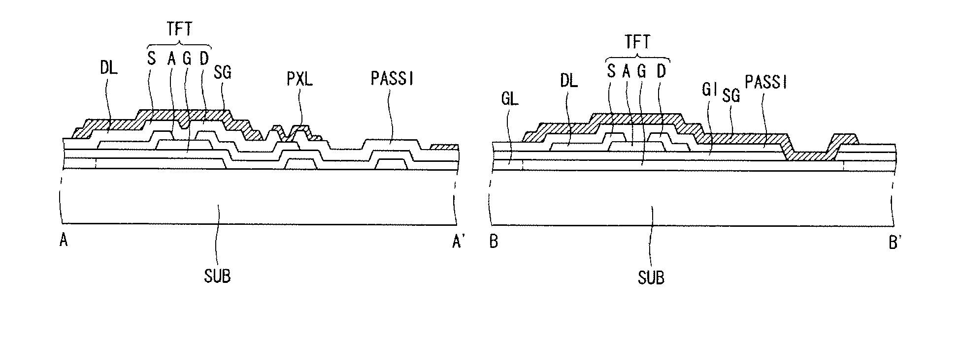
[0046]Referring to attached figures, we will explain preferred embodiments of the present disclosure. FIG. 4 a plane view illustrating a thin film transistor array substrate of the horizontal electric field type liquid crystal display device according to the present disclosure. FIG. 5 is a cross-sectional view illustrating the structure of the thin film transistor array substrate of FIG. 4 by cutting along the line A-A′. FIG. 6 is a cross-sectional view illustrating the structure of the thin film transistor array substrate of FIG. 4 by cutting along the line B-B′.

[0047]The horizontal electric field type liquid crystal display device according to the present disclosure comprises a thin film transistor array substrate TFTS having a plurality of thin film transistor TFT, a color filter array substrate (not shown) having a plurality of color filter (not shown), and a liquid crystal layer (not shown) disposed between the thin film transistor array substrate TFTS and the color filter arra...


PUM

PropertyMeasurementUnit
areaaaaaaaaaaa
conductiveaaaaaaaaaa
sizeaaaaaaaaaa

Abstract

The present disclosure relates to a liquid crystal display device having a protection element for semiconductor layer from externally intruding light and a manufacturing method of the same. The present disclosure suggests a liquid crystal display device comprising a substrate; a data line and a gate line crossing each other on the substrate; a thin film transistor formed at a crossing portion of the data line and the gate line; a passivation layer covering the thin film transistor; and an opaque protective layer forming on the passivation layer and covering the thin film transistor. The liquid crystal display device according to the present disclosure blocks the light intrusion into the semiconductor active layer of the thin film transistor to enhance the electron mobility in the active layer and the reliability of the elements.

Description

[0001]This application claims the benefit of Korea Patent Application No. 10-2009-0133559 filed on Dec. 30, 2009, which is incorporated herein by reference for all purposes as if fully set forth herein.BACKGROUND OF THE INVENTION[0002]1. Field of the Invention[0003]The present disclosure relates to a liquid crystal display device and a manufacturing method of the same. Especially, the present disclosure relates to a liquid crystal display device having a protection element for semiconductor layer from externally intruding light and a manufacturing method of the same.[0004]2. Discussion of the Related Art[0005]Nowadays, various flat panel display devices are developed for overcoming many drawbacks of the cathode ray tube such as heavy weight and bulk volume. The flat panel display devices include the liquid crystal display device (or LCD), the field emission display (or FED), and electroluminescence device (or ED).[0006]The liquid crystal display device represents video data by contr...

Claims


Application Information

Patent Timeline
Patent Type & Authority Patents(United States)
IPC IPC(8): G02F1/136
CPCG02F1/136209H01L29/78633H01L27/1259G02F1/136
Inventor KIM, YOUNGHOONYOON, JOONGMIN
Owner LG DISPLAY CO LTD
Features
  • R&D
  • Intellectual Property
  • Life Sciences
  • Materials
  • Tech Scout
  • Unparalleled Data Quality
  • Higher Quality Content
  • 60% Fewer Hallucinations
Learn More