Electrically erasable programmable read-only memory and manufacturing method thereof

a programmable read-only memory, electrically erased technology, applied in the direction of semiconductors, electrical apparatus, transistors, etc., can solve the problems of reducing the area of the manufacturing process of the eeprom, achieving a high coupling ratio, and complicated implementation and adoption of additional electronic circuits, etc., to achieve simple operation, easy to adapt, and simplify the effect of the peripheral circui

Active Publication Date: 2013-04-16
ELECTRONICS & TELECOMM RES INST
View PDF24 Cites 6 Cited by
  • Summary
  • Abstract
  • Description
  • Claims
  • Application Information

AI Technical Summary

Benefits of technology

[0008]Therefore, the present invention provides an EEPROM and a manufacturing method thereof in which a control gate is formed to enclose a floating gate except for the lower tunnel surface thereof to increase a coupling ratio in a same area thereby enabling low-voltage operation.
[0013]In accordance with the aspects of the present invention, the EEPROM apparatus is configured such that a control gate is formed to enclose all of a floating gate except for the lower tunnel surface of the floating gate. Hence, the coupling ratio is increased from about 72% to about 84% on the same area and the low-voltage operation becomes possible. Specifically, the coupling ratio may be increased on the same area and the area may be reduced by 50% at the same coupling ratio. Actually, such a high coupling ratio is applied, so that the voltage upon programming / erasing is decreased to about 12 V from the conventional 18 V, thus enabling the low-voltage operation.
[0015]Upon erasing, the control gate may prevent the generation of initial leakage current from the drain of the floating gate to the source when the floating gate transistor is “off” without floating the drain of the floating gate even in an over-erase state.
[0016]Therefore, thanks to the action of the control gate, the operational mode becomes simple and the operation is self-stabilized upon programming / erasing, whereby the peripheral circuit is simplified. Accordingly, the EEPROM in accordance with the present invention is easily adapted for embedded SoC applications, such as a smart card or an electronic apparatus, requiring a small amount of EEPROM.

Problems solved by technology

With the conventional EEPROM it is difficult to attain a high coupling ratio in proportion to an increase in its density, and thus requires high operating voltage for programming / erasing and needs a sophisticated electronic circuit using a time division procedure which is temporally precise and an intermediate verification algorithm for stable operation.
However, owing to sophisticated peripheral circuits and supply of high operating voltage, the manufacturing process of an EEPROM becomes simple and an area thereof gets reduced, whereby the EEPROM is widely employed in large-capacity chips.
As mentioned above, conventional EEPROM used in a small-scale for embedded system-on-chip (SoC) applications such as a smart card or a typical electronic apparatus should include an additional sophisticated electronic circuit to ensure a high operating voltage and stable operation thereof, but such an additional electronic circuit is complicated to be implemented and adopted.

Method used


Image

  • Electrically erasable programmable read-only memory and manufacturing method thereof
  • Electrically erasable programmable read-only memory and manufacturing method thereof
  • Electrically erasable programmable read-only memory and manufacturing method thereof

Examples


Embodiment Construction

[0021]Hereinafter, embodiments of the present invention will be described in detail with reference to an accompanying drawings form a part hereof.

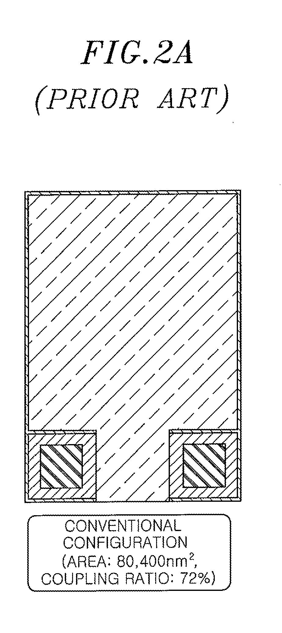
[0022]FIGS. 2A and 2B show layouts of same areas in the conventional EEPROM and an EEPROM in accordance with the present invention and coupling ratios thereof.

[0023]As shown in FIGS. 2A and 2B, the coupling ratios between a control gate and a floating gate of the configuration of the conventional EEPROM and that of the EEPROM in accordance with the present invention in a same area of 80,400 nm2 are 72% and 84% respectively. The EEPROM configuration in accordance with the present invention exhibits the area reduction effect of 50% compared to the conventional configuration at a same coupling ratio.

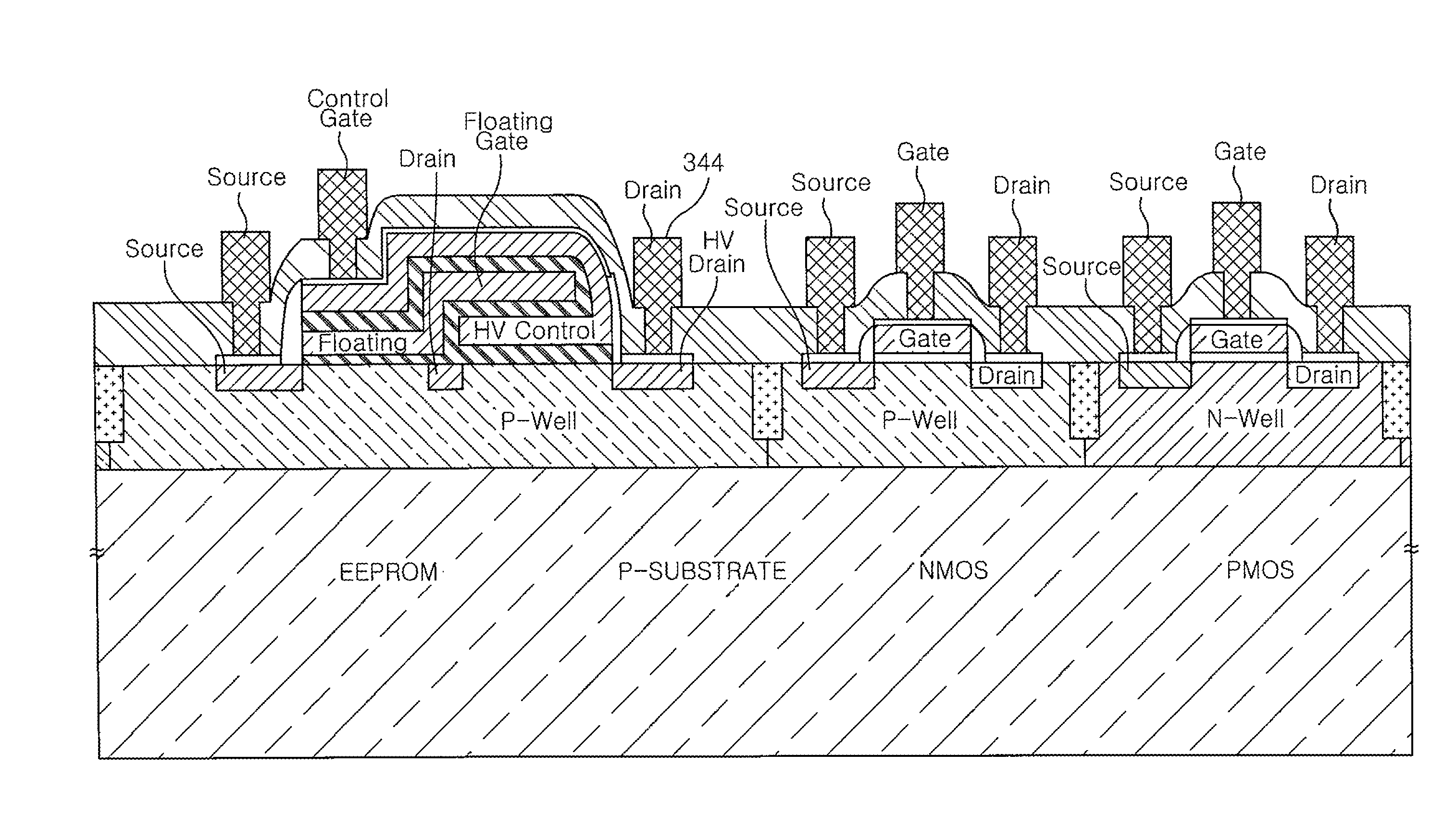
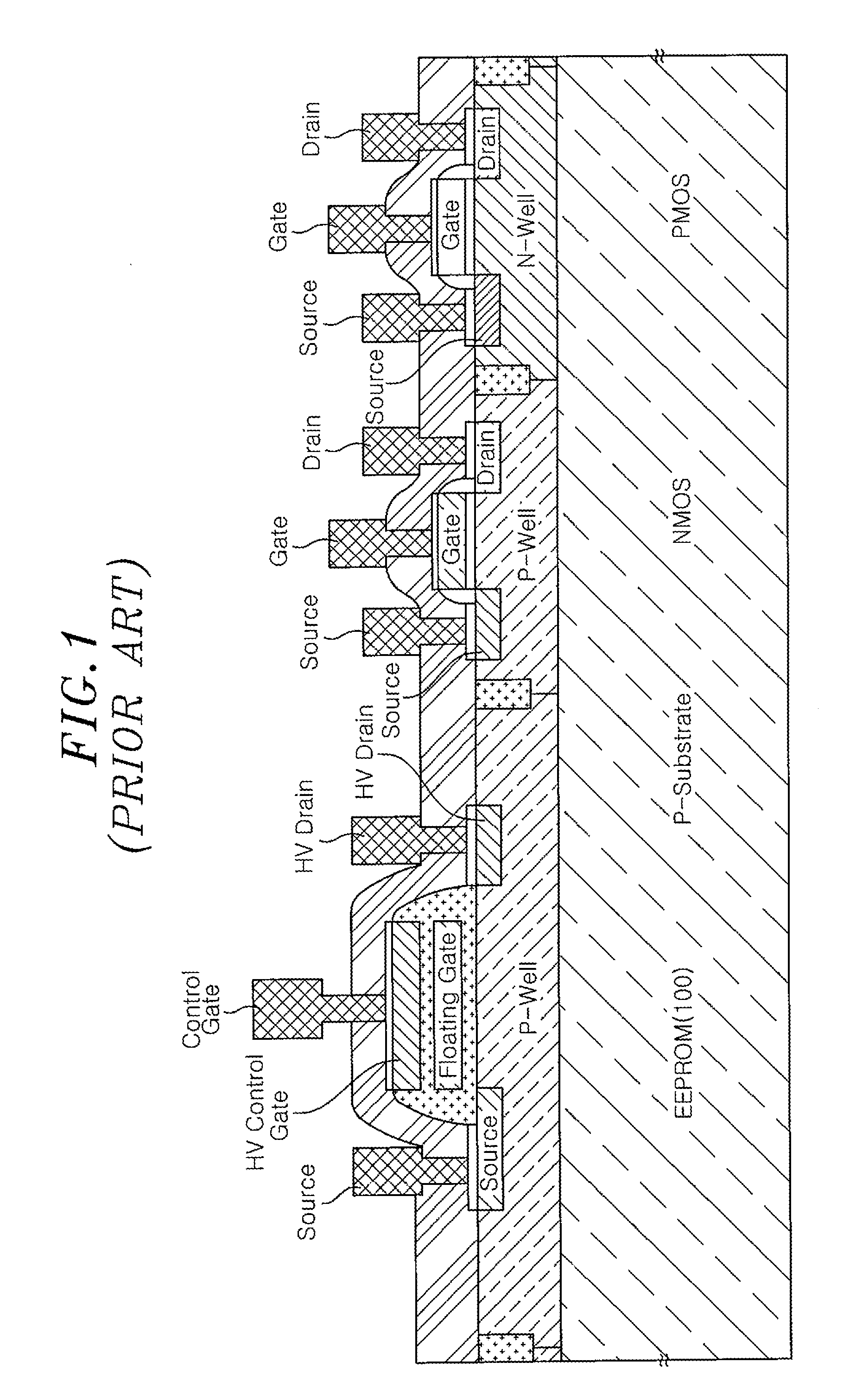
[0024]FIGS. 3A to 3M sequentially show an EEPROM manufacturing process in accordance with the embodiment of the present invention.

[0025]As shown in FIG. 3A, a p-type semiconductor substrate 300 which is a silicon wafer is doped with boron (B) ions...


PUM


Abstract

An electrically erasable programmable read-only memory includes a first polysilicon layer, a second polysilicon layer and a third polysilicon layer, the first polysilicon layer and the third polysilicon layer forming a control gate and the second polysilicon layer forming a floating gate. The first polysilicon layer is horizontally disposed in series with the second polysilicon layer and is connected to the third polysilicon layer, so that the control gate encloses all of the floating gate except for a tunnel surface of the floating gate.

Description

CROSS-REFERENCE(S) TO RELATED APPLICATION[0001]The present invention claims priority of Korean Patent Application No. 10-2009-0122676, filed on Dec. 10, 2009, which is incorporated herein by reference.FIELD OF THE INVENTION[0002]The present invention relates to a technique for manufacturing a semiconductor, and particularly to an electrically erasable programmable read-only memory (EEPROM) and a manufacturing method thereof in which a coupling ratio is increased in a same area thus enabling low-voltage operation thereof during programming / erasing and also in which a control gate connected in series to a floating gate is used to self-control the generation of excessive channel hot-electron (CHE) current upon programming and to suppress generation of initial leakage current resulting by a previous over-erase even if high voltage drain is not floated, whereby self-stabilizing operation of the EEPROM.BACKGROUND OF THE INVENTION[0003]In general, EEPROM cells in a semiconductor device exh...

Claims


Application Information

Patent Timeline
Patent Type & Authority Patents(United States)
IPC IPC(8): H01L29/788
CPCH01L21/28273H01L27/11521H01L29/7885H01L29/42324H01L27/11546H01L29/40114H10B41/49H10B41/30H01L21/265H01L21/823493
Inventor KANG, JIN-YEONG
Owner ELECTRONICS & TELECOMM RES INST
Why Eureka
Try Eureka